
A smart thermostat, air-quality node, or leak detector can pass bench checks and still drift after it is closed inside a warm plastic enclosure. The problem is usually not the sensing element alone. A regulator, status LED, radio burst, connector, and copper return path create a local thermal and electrical environment that the firmware later interprets as room data. This article follows a practical release path for a Smart Home PCB that must keep sensor placement, enclosure airflow, and calibration evidence aligned.
- Separate the sensor from heat-generating devices and copper paths.
- Keep the enclosure interface, board datum, and airflow assumptions visible in the layout.
- Build a calibration fixture that distinguishes board drift from environmental drift.
- Release thermal, assembly, and firmware changes as one controlled package.
Start with the enclosure heat map, not the sensor symbol
At schematic review, the sensor is often treated as a small block with a short I2C or SPI connection. The production problem starts when the physical board is placed next to a buck converter, a radio shield, or a bright indicator LED. Those parts can raise a local copper island or create a recirculating warm-air pocket. A Smart Home PCB should therefore carry an enclosure heat map that marks high-loss components, vent direction, mounting bosses, gasket compression, and the sensor’s no-copper or no-component region.
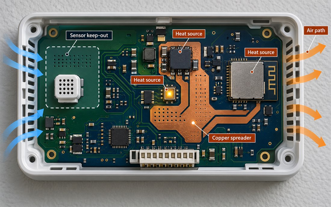
The keep-out is not an arbitrary circle. It should account for the sensor package, its port or vent, the connector shadow, and the thermal path through mounting hardware. The PCB layout should also prevent a high-current trace from running under the sensing element if that trace can modulate local temperature or magnetic fields. When the enclosure is revised, the board review must repeat this map rather than assuming the old clearance still works.
Decide which copper is allowed near the sensor
A large copper pour can spread heat away from a regulator, but the same pour can conduct heat toward a sensor. The decision depends on where the board is fixed, where the enclosure vents, and whether the sensor measures air, surface temperature, pressure, or gas concentration. Document the intended heat path and use a short note in the high-frequency PCB rules only when a nearby radio or clock edge makes return-current control relevant. The sensor zone and RF zone are related, but they are not the same design problem.
Control the electrical path that becomes a thermal path
Sleep current, radio burst current, and LED or actuator current can share a regulator but should not share every trace and via. A narrow neck between the battery entry and the radio can create avoidable voltage movement; a wide copper island below the sensor can create an avoidable thermal gradient. Treat the PCB manufacturing stackup, copper weight, and via pattern as part of the sensor design instead of leaving them to the last fabrication review.
For a battery node, place the load switch and bulk capacitor close to the radio supply pins, keep the sensor reference and analog return quiet, and route the current-shunt access point so it can be probed without lifting a component. The PCB assembly drawing should identify polarity, thermal relief, and any keep-out that prevents a shield or spring contact from touching the sensing area.
Use a release table that engineering and production can both read
| Release item | Engineering question | Production evidence |
|---|---|---|
| Sensor zone | Is the sensing port clear of heat and obstruction? | First-article photo and fixture datum check |
| Power path | Can the radio burst avoid the sensor reference? | Current-shunt access and assembly inspection |
| Enclosure | Does the vent and boss pattern match the board? | Mechanical overlay and sample fit |
| Calibration | Are reference conditions and firmware revision recorded? | Traveler entry and serialized result |
Do not turn a target value into a warranty. A design target such as a short settling interval or a limited local temperature rise is useful only when its fixture, ambient condition, and firmware revision are named. The PCB materials choice, solder mask, coating, and connector finish can shift the thermal response, so the release record should identify the approved material family and any allowed substitute.
Build calibration evidence around repeatable datums
A sensor calibration station becomes credible when the board is located the same way every time. Use a mechanical datum, a controlled reference source, a current-shunt position, and a defined cable or service connector. The fixture should isolate the board’s contribution from the chamber or reference instrument. This is where DFM review pays off: a test point that is easy to reach in the prototype may be hidden after panelization or blocked by a housing clip.
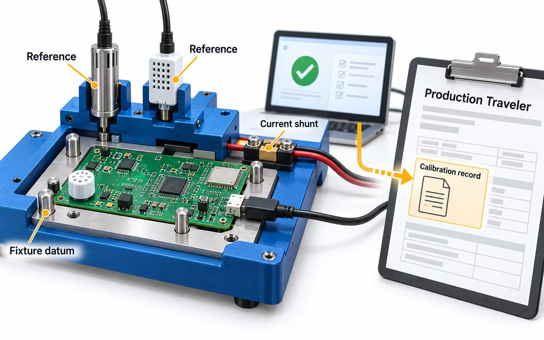
The assembly process should record board revision, sensor lot, firmware revision, fixture revision, and reference condition. If a later complaint shows a temperature or humidity offset, that chain lets the project manager separate a component-lot shift from a board-layout or enclosure change. The PCB fabrication traveler should also keep the panel drawing, copper balance notes, and coating instruction together.
What to review before an ECO is released
- Compare the old and new enclosure heat maps, not only the Gerber diff.
- Check whether a copper pour, via array, or shielding can now cross the sensor keep-out.
- Repeat the current-burst and sensor-settling sequence after regulator or radio changes.
- Verify that fixture datums and probe access survive the new panel outline.
- Link the approved RF return path rules to the enclosure and assembly review.
A robust Smart Home PCB release is not just a board file. It is a connected definition of sensor placement, power integrity, thermal path, enclosure fit, fixture method, and firmware assumptions. When those interfaces are reviewed together, a project can change the housing or radio without losing the ability to explain why a field reading moved.
For procurement, the decision is equally concrete: approve only the material, coating, assembly finish, and fixture configuration that the calibration record can identify. That approach keeps the approved PCB material list short, protects the sensor layout intent, and gives the manufacturing release a traceable basis.
Freeze the thermal assumptions at pilot release
For a Smart Home PCB, the pilot record should state the enclosure orientation, vent condition, sensor lot, and warm-up sequence. A later Smart Home PCB ECO is acceptable only when the same assumptions are rechecked against the new copper, coating, or component placement. This gives the project manager a visible handoff instead of a promise that the old calibration still applies.
Keep the Smart Home PCB reference fixture with the production traveler and identify which observations are targets versus measured readings. That small discipline prevents a thermal drawing from being mistaken for a customer test report.
Smart Home PCB release evidence for the enclosure team
The enclosure team should receive the Smart Home PCB sensor-zone drawing with the board datum, vent direction, and heat-source note. The electrical team should receive the Smart Home PCB power-path drawing with the probe access and approved substitute list. The production team should receive the Smart Home PCB fixture revision and calibration traveler together.
When the Smart Home PCB enters pilot build, the enclosure drawing, sensor keep-out, and fixture datum should travel with the same revision. If the Smart Home PCB uses a conformal coating, record the masked sensor port and the cure condition. If the Smart Home PCB changes its radio module, repeat the burst-current check before blaming the sensor. If the Smart Home PCB moves a connector, review the return path and cable shadow. Finally, the Smart Home PCB release owner should sign the calibration record only after the board, firmware, and fixture revisions agree.
Sources: Analog Devices low-power sensing and mixed-signal layout guidance; Würth Elektronik power, EMC, and assembly notes; Qorvo wireless integration references; sensor, regulator, connector, coating, and enclosure supplier application data. Values and checks above are engineering practices or design targets, not customer measurements.
