
Table of Contents
An IoT Sensor PCB can use a high-quality sensor and still report noisy or drifting values when the board couples digital current into the measurement path. The failure is common in gateways, condition-monitoring nodes, smart meters, and medical-adjacent instrumentation: the schematic is correct, but the return path, reference, connector, and assembly state were never released as one measurement system. Engineers need a layout that protects the signal before the data reaches the firmware. The release should also name the IoT Sensor PCB revision used for calibration.
Why a stable sensor gives unstable numbers
A sensor output may be only millivolts while a radio, display, or switching regulator moves amperes through nearby copper. If those currents share a narrow neck, the ADC sees ground movement as a false signal. Cable shields, mounting screws, and battery returns can create additional paths. A IoT Sensor PCB review should begin with the measurement error budget: identify the signal bandwidth, source impedance, ADC reference, expected noise, and the current events that must be isolated.
Do not start by drawing a large ground pour. First define the sensor front-end review: connector pins, protection, bias, gain, filtering, and ADC entry. Place the sensor and its first conditioning stage close together, then decide how the return reaches the quiet reference. A short trace is not automatically quiet if it crosses a switching return or a split plane.
Build the analog path for an IoT Sensor PCB before the digital path
Keep the high-impedance node short, guard it from fast digital traces, and provide a defined path for input bias current. The anti-alias filter should be located where it can be inspected and changed without moving the sensor datum. If an instrumentation amplifier is used, route both inputs as a matched pair through the same environment. The analog ground plane should support the sensor and ADC reference without forcing return current through a connector shield or a processor ground neck.
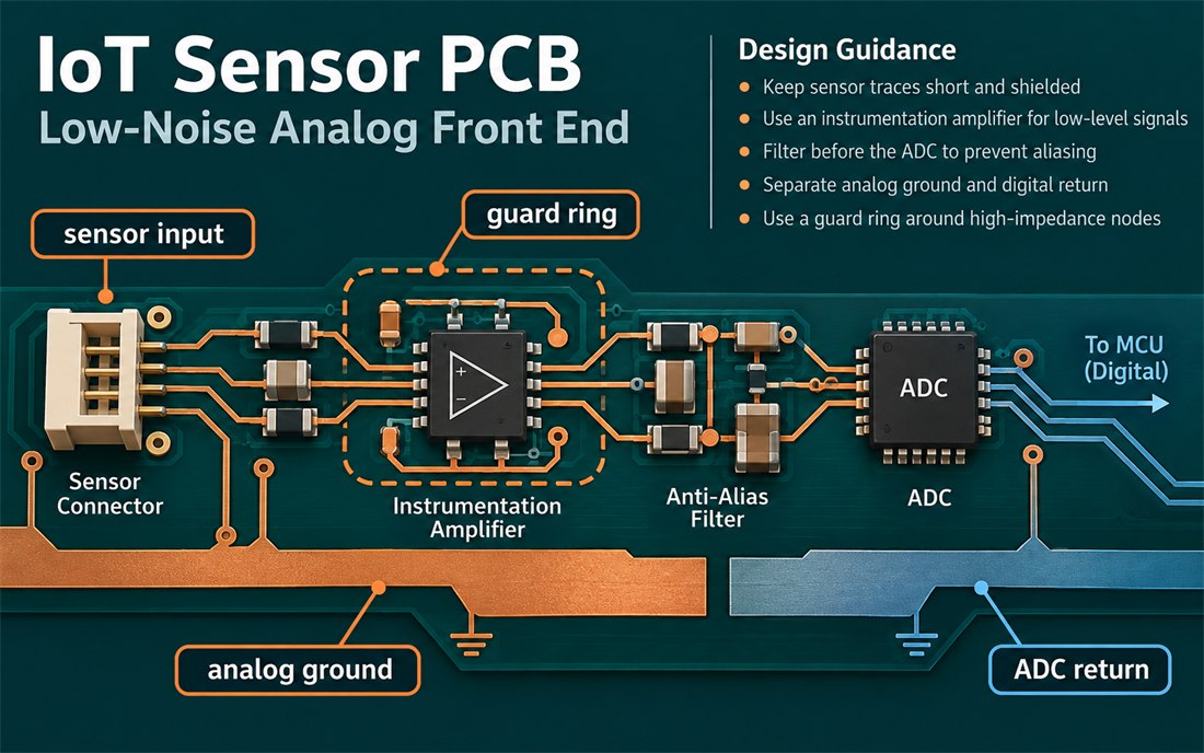
This conceptual figure shows a sensor input, amplifier, filter, ADC, analog ground, and guard ring. It is an explanation of layout intent, not a measured noise plot. For a production IoT Sensor PCB, lock the layer stack and copper construction before tuning. A change in dielectric thickness or plane reference can alter both impedance and coupling, even when the schematic is unchanged.
Use boundaries that a manufacturer can inspect
Mark the sensor keep-out, guard ring, test pads, and quiet-zone boundary on the fabrication or assembly drawing. The guard-ring detail should state where copper is allowed and where solder mask must remain intact. If the sensor connector is near a board edge, separate its shield from the analog return unless the interface drawing intentionally bonds them. A shielded sensor-cable plan should show the entry point, chassis contact, and protection path.
Treat an IoT Sensor PCB ground and references as measurement structures
The ADC reference on an IoT Sensor PCB is part of the measurement, not an accessory. Place its decoupling at the reference pins, isolate it from converter pulses, and route the return without a shared via barrel that carries radio current. Define a reference-plane construction that the fabricator can hold, and inspect the relevant copper and via transitions at first article.
Use a noise budget that distinguishes sensor noise, reference noise, regulator ripple, digital edge coupling, and quantization. The ADC reference review should record which terms are design targets and which are measured. This prevents a project team from hiding a process change inside a firmware filter. If the radio transmits during sampling, define whether the sample is rejected, synchronized, or protected by a quiet power state.
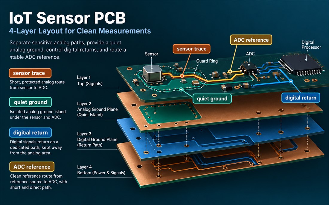
The second conceptual figure separates sensor trace, quiet ground, digital return, and ADC reference. It should not be presented as a customer measurement. A noise-budget worksheet and a via-transition inspection make the intended current paths visible to design, fabrication, and test teams.
Keep accuracy through assembly
Component placement, solder volume, cleaning, and rework can change a sensor node. A thermally stressed package may shift offset; residue under a high-impedance input can create leakage; a shield can can press against a sensitive trace. Define the calibration-fixture interface with board support, probe access, connector orientation, and software revision. The first article should record the build state used for calibration, not only the final numerical correction.
Protect the sensor opening, membrane, or optical window during cleaning and coating. If a process supplier changes chemistry, review the sensor manufacturer’s compatibility guidance and the board’s keep-out. A rework boundary should identify which components may be replaced and which calibration must be repeated afterward.
Make the calibration state reproducible
Calibration is only comparable when the fixture, supply voltage, warm-up time, sensor stimulus, and firmware build are controlled. A project team should define which offset and gain terms are corrected in software and which indicate a board or assembly problem. Probe pressure can also matter on high-impedance nodes, so the fixture should contact approved test pads rather than exposed sensor pins. Record the board orientation and cable routing used during the first article. If the sensor vendor, ADC reference, or connector changes, repeat the uncertainty review before reusing old limits. This gives purchasing and manufacturing a clear decision path without claiming a universal accuracy result.
Release a repeatable measurement board
- Freeze the sensor datum, connector, analog path, ADC reference, and radio activity state.
- Show the guard ring, analog return, digital return, shield bond, and test points on controlled drawings.
- Label typical values, design targets, engineering ranges, and measured values separately.
- Define stackup, copper, via, solder-mask, cleaning, coating, and assembly support assumptions.
- Use a first-article release package with inspection and calibration records.
- Route sensor, regulator, connector, or firmware changes through a controlled calibration change review.
When the current paths and calibration state are controlled, an IoT Sensor PCB becomes a repeatable measurement platform instead of a board that depends on one engineer’s bench setup. For an IoT Sensor PCB, the objective is not to promise a universal accuracy number; it is to make every contributor to the measurement visible, inspectable, and recoverable during production.
Sources: Analog Devices mixed-signal grounding and ADC layout guidance; Würth Elektronik sensor and RF layout notes; Qorvo front-end integration guidance; laminate and assembly supplier technical data. Values above are engineering practices or design targets, not customer measurements.
