
A connector launch is the shortest section of a Ku-band channel and one of the easiest to release incorrectly. A PTFE PCB can provide a stable low-loss path, but the launch still depends on pin geometry, pad shape, antipad, ground-via placement, solder mask, and the first bend. A project team may see a clean schematic and a correct stackup while the assembled launch contains a resonant discontinuity that consumes the RF margin.
Lock the launch datum before routing the board
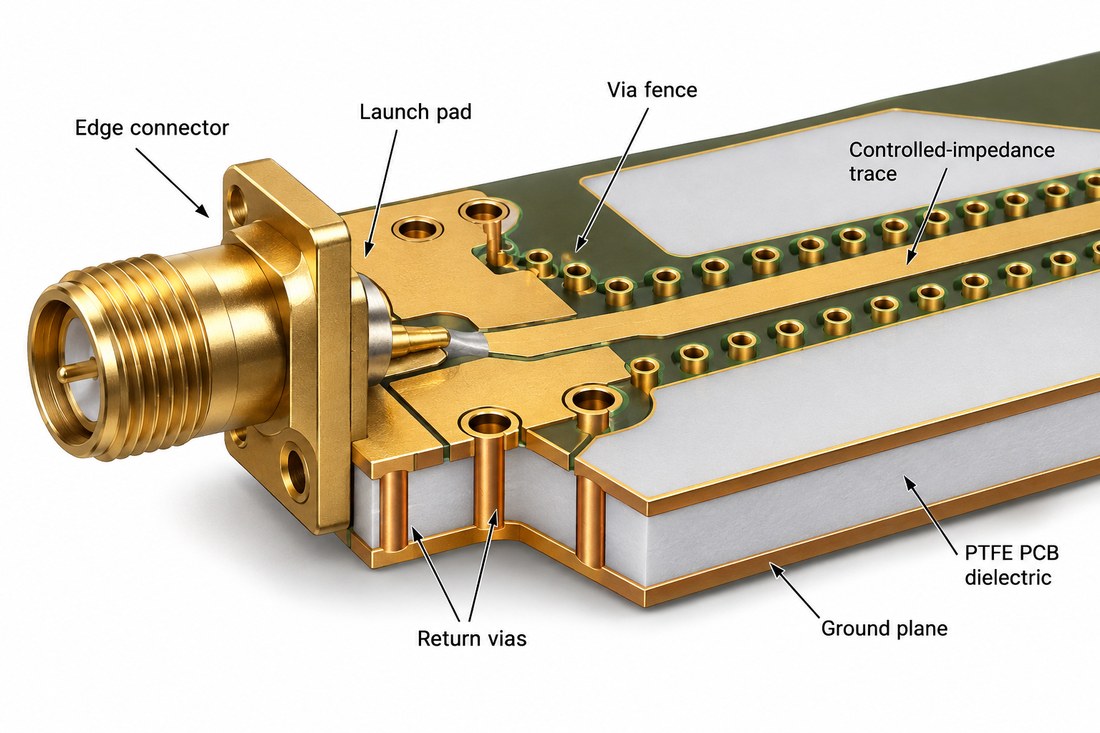
Create a launch drawing that references the connector body, pin, board edge, and first controlled section. The PTFE PCB stackup should show the dielectric thickness used by the launch field model, not only the total board thickness. If the connector vendor offers several footprint variants, record the selected footprint and revision in the PCB release.
Use a continuous ground return around the signal pin. Analog Devices guidance notes that a layer transition benefits from nearby ground vias and a low-inductance return. The RF PCB layout should therefore define a via pattern, keep-out, and drill tolerance instead of leaving the return to a general ground-pour rule.
Keep the first bend and component pad outside the connector’s near field unless the field model includes them. A solder mask opening or a copper neck can change the local capacitance enough to make a launch look like a material failure.
Make back-drill and plating assumptions explicit
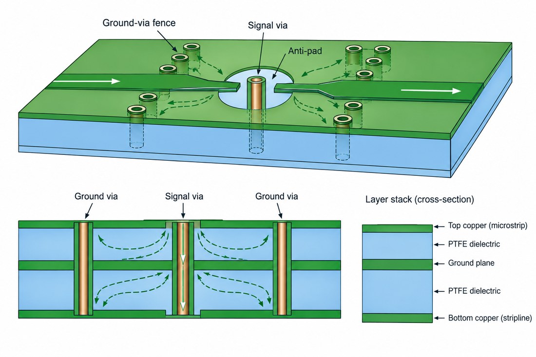
Unused via stubs can create a discontinuity when a high-frequency line changes layers. If back-drilling is used, specify the stub target, drill depth reference, tolerance, and the treatment of the remaining barrel. The PTFE PCB fabrication drawing should also state whether the via is through, blind, buried, filled, or mechanically drilled after plating.
The controlled impedance manufacturing note should distinguish the designed back-drill depth from the process capability window. A generic back-drill statement cannot prove the residual stub for every connector location. Add a witness or cross-section plan where the stub is a release risk.
After assembly, inspect connector coplanarity, solder fillet, shield contact, and ground-via continuity. A launch coupon is useful only when its stack and footprint represent the production interface.
Plan the verification loop
Use a consistent calibration and fixture plan for launch correlation. Record which result is a design target, which is an engineering range, and which is a measured sample result. The thermal management release package should retain the sample ID and board revision whenever the data informs a go/no-go decision.
When a connector vendor changes the pin length or plating, re-open the launch review even if the footprint name is unchanged. A small mechanical change can move the reference plane or alter the solder geometry.
Close with a launch checklist: connector revision, stackup, pad and antipad, ground-via pattern, back-drill note, solder mask, coupon, and calibration method. This keeps the RF and manufacturing teams aligned.
A PTFE PCB launch is a complete three-dimensional transition, not a pad copied from a library. Release the connector, stackup, return path, and back-drill evidence as one controlled feature.
Implementation note for this connector launch and via transition review: keep the engineering assumption visible at the point where it affects a drawing, a supplier quote, or an inspection record. Ask the design owner to identify the reference plane, interface datum, and acceptance method before the release is frozen. Ask manufacturing to return the proposed stack, panel, and process window rather than a generic capability statement. Ask assembly to identify the profile, cleaning, and support conditions that could move the RF or thermal result. This simple handoff prevents a typical material value from being mistaken for a guaranteed product result and gives the project team a clear action when an ECO changes the physical boundary.
Release note: freeze the PTFE PCB connector datum, via geometry, and return path in the released drawing so a supplier change cannot move the RF reference plane.
Additional release check: keep the PTFE PCB connector datum and via-return assumption tied to the approved drawing before the next ECO.
Sources: Panasonic MEGTRON technical material guidance; Rogers and Taconic high-frequency material data sheets where relevant; CeramTec ceramic substrate data; Analog Devices RF and mixed-signal layout guidance. Numerical values are treated as typical supplier values or engineering targets unless the released drawing defines a measured acceptance value.
Release note: confirm the PTFE PCB construction before the next ECO.
Release note: confirm the PTFE PCB construction before the next ECO.
Release note: confirm the PCB manufacturing evidence before approval.
Release note: confirm the PCB assembly evidence before approval.
