
A ceramic substrate can be electrically stable and thermally efficient while the interconnect still becomes the weak point. Metallization adhesion, plated or filled vias, copper thickness, and the transition to a connector or carrier all experience different mechanical strain. For a Ceramic PCB used in a power or microwave module, the correct question is not whether a via works in a schematic. It is whether the selected via technology, copper interface, and thermal cycle remain compatible over the life of the product.
Table of Contents
- Separate the electrical and mechanical roles of each metal feature
- Design for thermal-cycle strain
- Release inspection and change control
Separate the electrical and mechanical roles of each metal feature
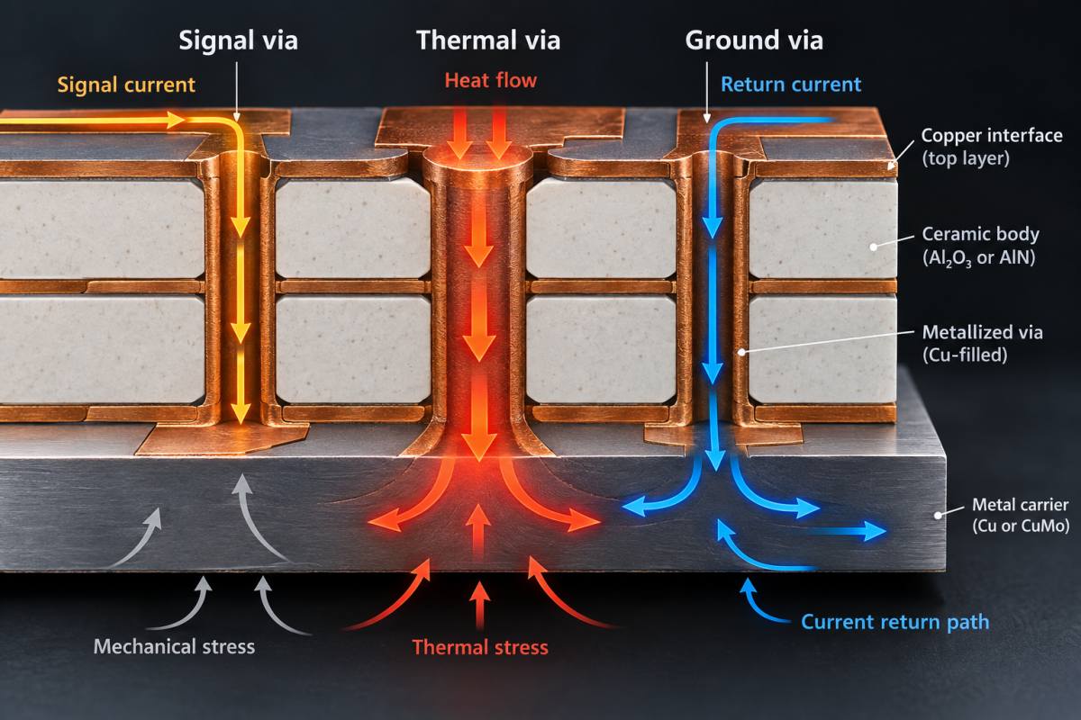
Create a feature map for signal vias, thermal vias, ground vias, mounting holes, and carrier bonds. A Ceramic PCB may use several metallization systems in one assembly, and each one has its own adhesion and inspection method. The drawing should show which features are part of the RF circuit and which are only mechanical or thermal.
For a signal transition, define pad diameter, barrel or filled-via condition, antipad, and the nearest return features. For a thermal array, define the fill or attach method, void allowance, and the interface to the heat spreader. The RF PCB specification should not use one generic via note for every feature because a manufacturing change that is harmless to a thermal via can be damaging to a high-frequency launch.
Use supplier data as a starting point and make the acceptance criteria measurable. If a thermal conductivity number is typical, do not turn it into a guaranteed junction temperature. If adhesion is critical, specify the test method or inspection evidence required for the release.
Design for thermal-cycle strain
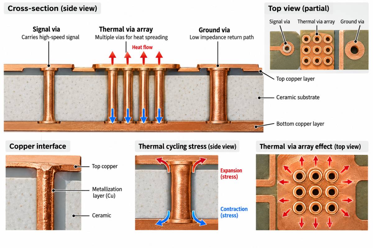
Ceramic, copper, solder, and metal carriers do not expand at the same rate. A rigid interface can concentrate stress at a via corner, an edge metallization, or a solder fillet. The Ceramic PCB drawing should identify compliant regions, keep-out distances, and the expected neutral axis when a board is mounted to a carrier.
The controlled impedance review should compare the stack CTE assumptions with the assembly profile and the enclosure constraint. Use a coupon or cross-section plan to examine the actual interface after the first build. A coupon is evidence of the sampled process, not proof that every future board will behave identically.
Where a high-current path enters the ceramic, spread the current before it reaches a small neck or isolated pad. Keep RF ground stitching close to the launch, but avoid forcing ground and power vias into the same stress concentration without a mechanical review.
Release inspection and change control
A reliable production package names the critical dimensions, their datums, and the evidence returned with each lot. Include metallization continuity, via fill or plating condition, copper thickness, flatness, and the carrier interface. The thermal management handoff should state whether a cosmetic chip is acceptable, when a crack is rejectable, and how rework is recorded.
If the supplier proposes a different paste, plating, or copper foil, treat it as a controlled change. Recalculate the RF geometry and thermal path instead of approving the change under a general equivalent-material statement. Keep the Ceramic PCB material identifier and revision in the bill of materials and drawing title block.
For the project gate, review the feature map, thermal-cycle plan, cross-section locations, and lot traceability together. This turns ceramic via reliability from a supplier assumption into a deliverable that engineering, quality, and procurement can share.
The strongest Ceramic PCB release is explicit about every metal interface. Separate signal, thermal, ground, and mechanical features, connect them to measurable evidence, and control substitutions before they reach a production lot.
Implementation note for this metallization and via reliability review: keep the engineering assumption visible at the point where it affects a drawing, a supplier quote, or an inspection record. Ask the design owner to identify the reference plane, interface datum, and acceptance method before the release is frozen. Ask manufacturing to return the proposed stack, panel, and process window rather than a generic capability statement. Ask assembly to identify the profile, cleaning, and support conditions that could move the RF or thermal result. This simple handoff prevents a typical material value from being mistaken for a guaranteed product result and gives the project team a clear action when an ECO changes the physical boundary.
For this Ceramic PCB via review, record the signal, thermal, and ground feature classes separately so a supplier change can be assessed against both reliability and RF continuity.
The Ceramic PCB metallization release should separate signal, thermal, and mechanical features so process changes remain reviewable.
A second Ceramic PCB metallization review should show the evidence for adhesion, via condition, copper thickness, and the related change trigger.
Sources: Panasonic MEGTRON technical material guidance; Rogers and Taconic high-frequency material data sheets where relevant; CeramTec ceramic substrate data; Analog Devices RF and mixed-signal layout guidance. Numerical values are treated as typical supplier values or engineering targets unless the released drawing defines a measured acceptance value.
Release note: confirm the Ceramic PCB construction before the next ECO.
Release note: confirm the PCB manufacturing evidence before approval.
Release note: confirm the PCB assembly evidence before approval.
