
Connector launches often become the hidden bottleneck in a high-speed program. The laminate may have a low loss tangent, but an unused barrel stub, a broken reference plane, or an asymmetric ground-via pattern can dominate the transition. Treat every Megtron 7 PCB as a small RF structure with its own geometry, datum, and verification plan.
Map the connector launch
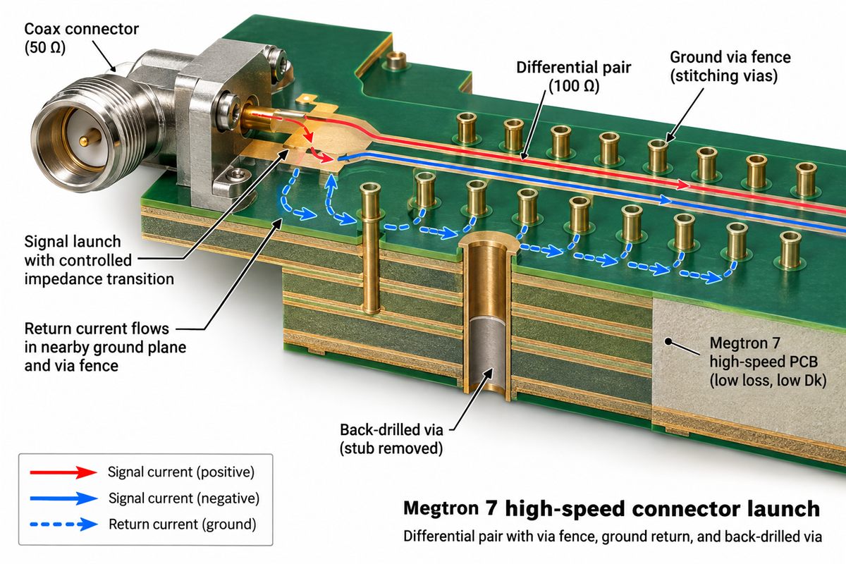
Begin with the connector manufacturer’s pin field, recommended antipad, and mating interface. Then map the signal path from the connector pad to the first controlled stripline or microstrip section. Mark every change in reference plane, via diameter, pad shape, and dielectric thickness. The goal is not to make the launch look symmetrical on a drawing; it is to keep the signal and return currents close through the entire transition.
Panasonic positions MEGTRON 7 grades for high-speed and large-format multilayer boards. Its typical low-Dk/Df values can help the transmission-line portion, but they do not remove launch discontinuity. A high-speed PCB layout review should therefore include the connector footprint, antipad, stitching-via pitch, and the first bend after breakout. Keep the breakout short and avoid routing a differential pair through a changing plane opening.
Control via and back-drill geometry
A plated through via that continues below the active layer becomes a stub. At a sufficiently fast edge, that stub can reflect energy even if the nominal bit rate appears moderate. Define the back-drill start and stop layers from the finished stackup, not from the artwork file alone. Account for drill wander, residual stub, copper thickness, and the tolerance of the mechanical drilling process.
Ground vias are part of the launch, not optional decoration. Place them so the return path does not jump across a split plane or detour around a large antipad. When the connector uses a shield or press-fit shell, keep the board ground strategy consistent with the assembly drawing. The PCB fabrication review should check drill tables, back-drill notes, plating sequence, and the reference datum used by inspection.
For dense boards, a sequential-lamination or HDI transition may replace a long through via. In that case, document which microvia, buried via, or through via carries the signal and how the return plane is stitched. A Megtron 7 PCB keeps the electrical intent aligned with actual process limits.
Verify the transition at release
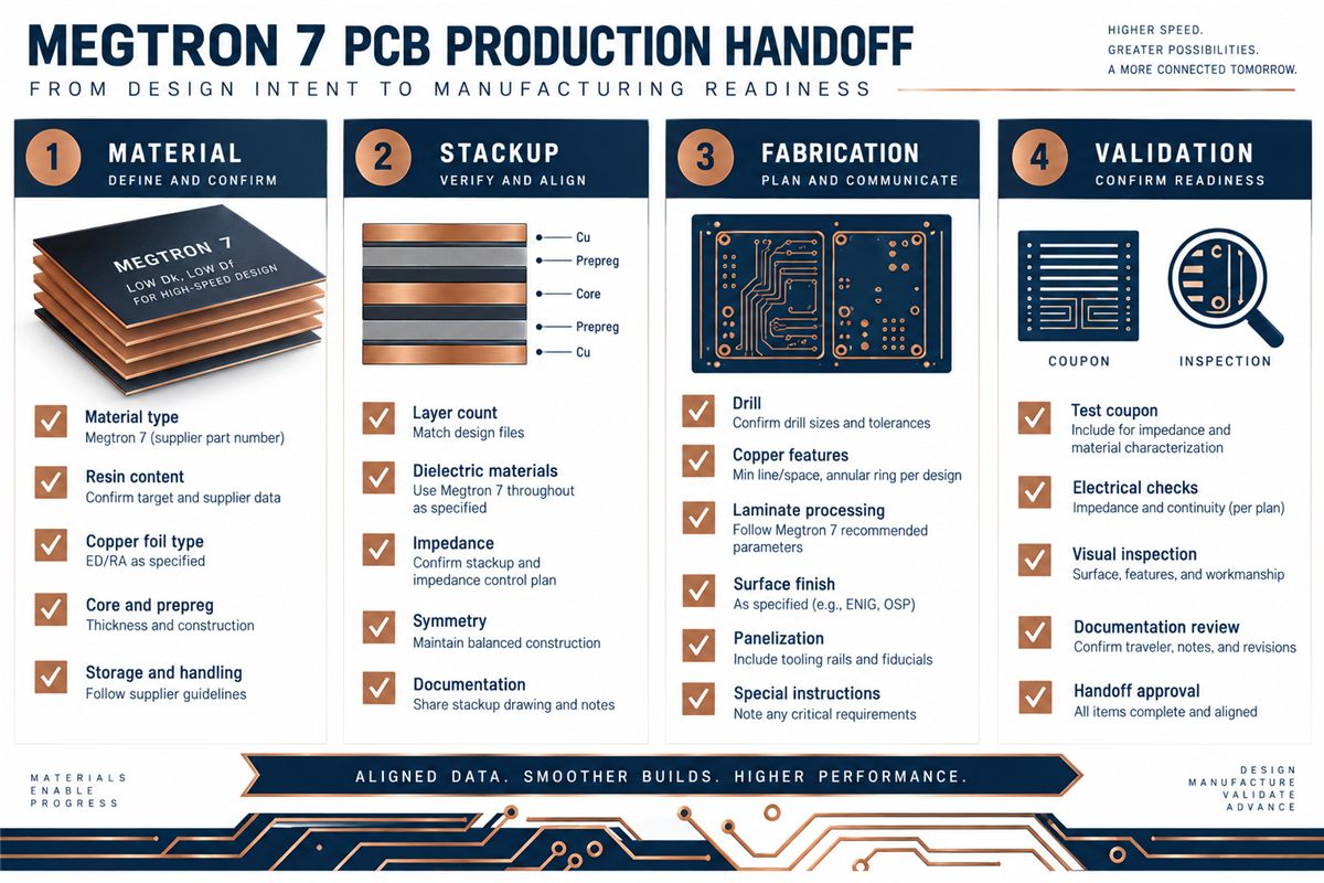
Use a coupon that represents the launch geometry when the connector is the dominant risk. A simple straight-line coupon can verify impedance but may not reveal a poor antipad or return-via arrangement. Define the acceptance method, fixture, and calibration reference before requesting a report. Any number shown in a concept review should be labeled as a target or engineering estimate rather than a measured customer result.
KKPCB can align the PCB material construction with the connector’s dielectric environment and coordinate the PCB assembly process so press-fit force, solder fillet, and connector coplanarity do not shift the launch. For complex ports, use Megtron 7 PCB and keep the released launch drawing under ECO control. Add a Megtron 7 PCB launch model.
The final checklist is short: reference planes are continuous, signal and return vias are paired, residual stubs are controlled, back-drill tolerances are stated, and the coupon matches the product transition. Keep a back-drill fabrication note in the released drawing. Keep a back-drill fabrication note in the released drawing. Keep a back-drill fabrication note in the released drawing. With those controls, a Megtron 7 PCB is a manufacturable interface rather than a last-minute tuning exercise.
Add a connector inspection plan and a return-path review to the launch package.
Add a and a to the launch package.
Sources: Panasonic MEGTRON 7 material data and KKPCB high-frequency, PCB layout, HDI, and manufacturing capability pages. Transition limits and acceptance values should be confirmed against the released stackup and connector drawing.
