
A TLY-5 PCB via field is not a cosmetic layout detail in a Ku-band module. The plated transition decides where the return current closes, how much barrel remains beyond the active layer, and whether the connector launch modeled by the RF team still represents the finished board. When this is released late, the first prototype can become a tuning exercise instead of a controlled engineering comparison.
RF engineers usually see the problem as a shifted resonance, excess insertion loss, or channel-to-channel phase spread. Project managers see it as a loop between layout, fabrication, assembly, and test. This article isolates the transition decisions that make a TLY-5 PCB via field repeatable without hiding a geometry problem behind a last-minute tuning notch. The TLY-5 PCB via field is a release feature, not a late tuning patch.
Table of Contents
TLY-5 PCB via field: lock the launch datum
Start from the connector or package datum. Dimension the signal pad, anti-pad, reference-via row, solder-mask opening, and board edge from one coordinate system. On a short RF launch, a small edge-registration shift changes the spacing between signal and return vias. The mechanical change may look minor on a drawing while the electrical effect appears as a different phase slope.
TLY-5 typical data is often described around Dk 2.20 with low Df near 0.0009. Those are useful starting values for a field-solver model, not a finished-board guarantee. The stackup should record the finished dielectric target, copper thickness assumption, and the layer pair used by the transition. Avoid mixing a nominal catalog value with a press thickness that has not been defined for production.
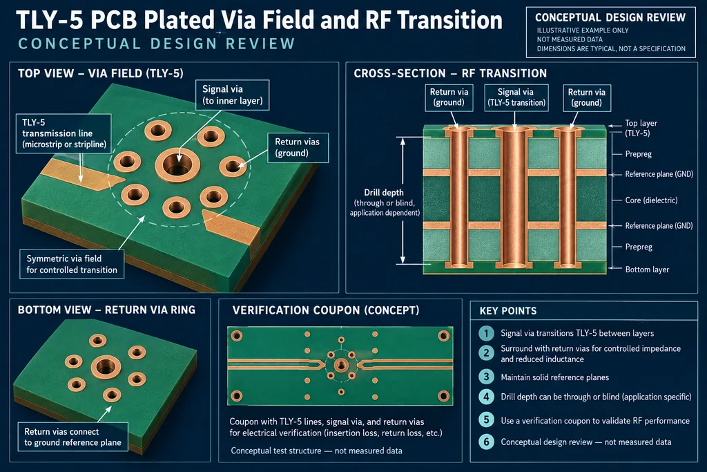
Design the return-current path, not just the signal barrel
A via fence only helps when its return plane is continuous through the launch. Splits, clearance pockets, connector keep-outs, and isolated copper islands can force the current to detour. Review the top layer, the cross-section, and the return-plane anti-pad as one feature. The released controlled-impedance PCB drawing should state finished hole, signal-via diameter, anti-pad diameter, return-via pitch, and connector-ground spacing.
Use a short blind or back-drilled transition only when it solves a defined bandwidth or stub problem. More advanced drilling adds depth control, registration, inspection, and yield dependencies. A simulated transition can still correlate poorly if the plated barrel or remaining stub falls outside the modeled window.
Model plated geometry and residual stubs
Plating changes the finished hole and barrel surface, while layer registration changes the copper remaining around an anti-pad. A through-via may leave a stub on an unused layer; a depth-controlled structure may trade stub reduction for a tighter process window. The decision should be tied to the frequency band and measured correlation plan rather than to a preferred feature name.
The PCB manufacturing traveler should carry drill class, plating requirement, back-drill or depth-control instruction, cross-section, and inspection datum. Keep the laminate, copper profile, and surface finish in one RF PCB material revision so a material change is not mistaken for a via failure.
Build a representative coupon
A generic impedance strip can monitor a process, but it cannot reveal whether a connector launch is centered, whether a stub remains, or whether the return fence is registered to the same datum. Put a witness structure on the same panel using the same layer pair, drill sequence, copper density, and finish. Its purpose is correlation to the product transition, not decoration.
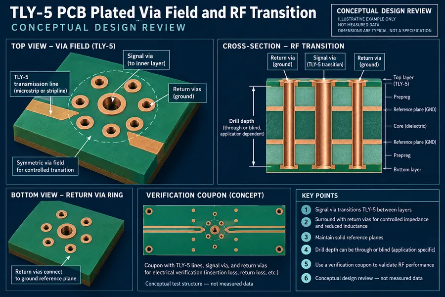
Before assembly, inspect hole size, annular ring, anti-pad registration, and copper balance. During PCB assembly, protect the launch from unnecessary rework. Connector placement, solder fillet geometry, cleaning limits, and rework disposition belong in the RF handoff because they can move the reference plane after the bare board has passed.
Gate the TLY-5 PCB via field as a controlled release feature
A useful release gate answers seven questions: Is the mechanical datum locked? Is the finished dielectric target recorded? Are signal and return vias dimensioned? Is the stub strategy explicit? Does the coupon represent the product? Are connector placement and solder acceptance defined? Is the VNA reference plane documented? This turns “RF launch risk” into evidence that a project manager can schedule.
KKPCB’s high-frequency PCB review can focus on those dimensions instead of reopening the complete layout. The final PCB manufacturing package should distinguish typical material values, calculated design targets, and measured acceptance data. If a value is not measured, label it as a target and preserve the assumption.
Keep the TLY-5 PCB material decision tied to the finished board, not only the datasheet. The TLY-5 PCB field model, TLY-5 PCB impedance review, and TLY-5 PCB drill acceptance should share the same datum and stackup revision.
Sources: Taconic TLY-5 typical material data; IPC-TM-650 methods relevant to drilling, plating, registration, and impedance; RF application guidance from Qorvo and Analog Devices; KKPCB PCB design, materials, manufacturing, assembly, and high-frequency capability pages. Values are typical, target, or calculated references unless explicitly identified as measured.
