1. The Rapid Growth of 5G Router PCB Technology
The expansion of:
- 5G wireless communication
- High-speed internet infrastructure
- Smart home networking
- Industrial IoT systems
- AI-connected devices
has significantly increased demand for advanced 5G Router PCB solutions.
Modern 5G routers require PCB systems capable of supporting:
- High-frequency RF transmission
- Multi-antenna communication
- Ultra-fast data processing
- Low latency networking
- Stable wireless connectivity
Compared with traditional networking equipment, 5G routers operate at:
- Higher frequencies
- Greater bandwidths
- Faster transmission speeds
This creates major PCB design challenges involving:
- Signal integrity
- RF interference
- Thermal management
- Controlled impedance routing
At KKPCB, advanced 5G router PCB solutions are engineered for:
- High-speed wireless communication
- Stable RF performance
- Low-loss signal transmission
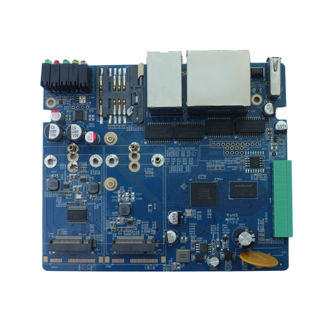
2. What Is a 5G Router PCB?
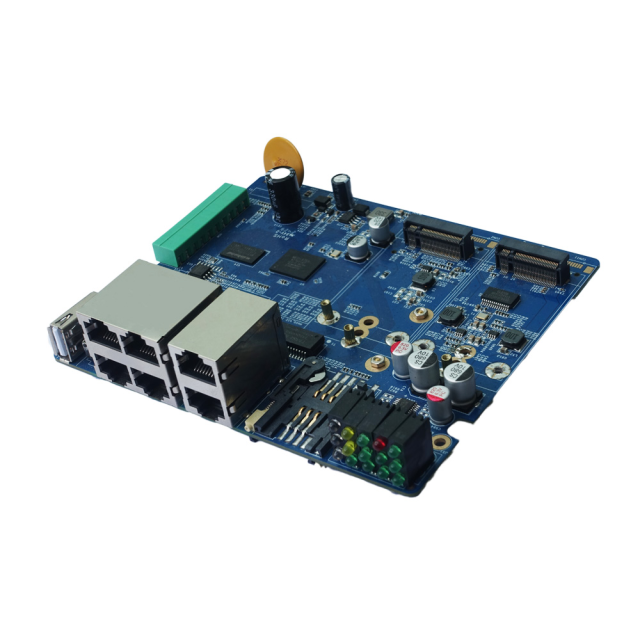
A 5G Router PCB is a high-frequency multilayer printed circuit board specifically designed for:
- 5G wireless communication systems
- High-speed networking equipment
- RF antenna integration
- High-bandwidth data transmission
5G router PCB structures typically integrate:
- RF transceiver circuits
- Antenna arrays
- High-speed processors
- Power management modules
- Ethernet and Wi-Fi communication interfaces
These PCB systems must provide:
- Stable RF signal transmission
- Excellent signal integrity
- Efficient heat dissipation
- Reliable high-speed operation
3. Key Design Challenges of 5G Router PCB
3.1 High-Frequency Signal Transmission
5G communication operates at extremely high frequencies.
This increases sensitivity to:
- Signal loss
- RF reflection
- Transmission discontinuities
- Crosstalk interference
5G router PCB design must minimize:
- Insertion loss
- Signal attenuation
- High-frequency distortion
3.2 Controlled Impedance Routing
Controlled impedance is essential for:
- RF communication stability
- High-speed data transmission
- Antenna matching accuracy
Key impedance-controlled structures include:
- Differential pair routing
- RF microstrip lines
- Stripline routing
Characteristic impedance depends on PCB transmission structures:
Z0=LCZ_0 = \sqrt{\frac{L}{C}}Z0=CL
At KKPCB, impedance-controlled multilayer PCB designs optimize:
- RF transmission efficiency
- Signal integrity
- Wireless communication stability
3.3 Signal Integrity Optimization
Signal integrity is critical for maintaining:
- High-speed communication quality
- Stable data transmission
- Reliable network performance
Signal integrity challenges include:
- Reflection loss
- Timing skew
- EMI interference
- Crosstalk noise
Optimization techniques include:
- Short high-speed routing paths
- Ground via stitching
- Reference plane continuity
- Differential pair matching
3.4 Thermal Management
5G routers generate substantial heat from:
- High-speed processors
- RF power amplifiers
- Network switching ICs
- Power management systems
Thermal management solutions include:
- Thermal via arrays
- Copper heat-spreading planes
- Heat sink integration
- Airflow optimization
Proper thermal design improves:
- System stability
- Wireless performance
- Long-term reliability
4. PCB Materials for 5G Router PCB
Material selection strongly impacts:
- RF signal quality
- High-frequency loss
- Thermal performance
Common 5G PCB materials include:
- Low-loss FR4
- Rogers RF laminates
- PTFE-based high-frequency materials
- Hydrocarbon ceramic laminates
These materials provide:
- Low dielectric loss
- Stable dielectric constant
- Reliable RF transmission performance
5. Multilayer Stack-Up Design for 5G Router PCB
Modern 5G router PCB structures typically use:
- Multilayer PCB architectures
- HDI PCB technology
- Dedicated RF layers
- Independent power and ground planes
Proper multilayer stack-up improves:
- Signal isolation
- EMI suppression
- Controlled impedance stability
- High-density routing capability
6. RF Antenna Integration in 5G Router PCB
Antenna integration is one of the most critical aspects of 5G router PCB design.
Modern 5G routers often use:
- MIMO antenna systems
- Beamforming technology
- Multi-band RF structures
PCB layout optimization improves:
- Antenna efficiency
- RF signal coverage
- Communication stability
Important RF design techniques include:
- Isolation between antennas
- Controlled RF trace routing
- Ground plane optimization
- RF shielding structures
7. EMI and EMC Control in 5G Router PCB
High-speed RF systems generate significant electromagnetic interference.
EMI control strategies include:
- Ground shielding
- Via stitching
- Signal isolation
- Filter integration
- Controlled return current paths
Effective EMI suppression improves:
- RF stability
- Wireless communication quality
- Regulatory compliance performance
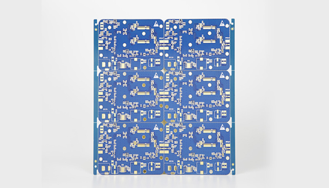
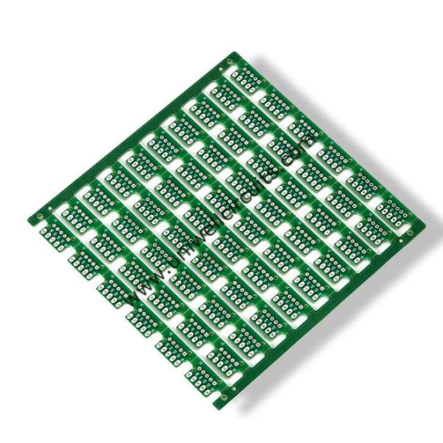
8. Manufacturing Challenges of 5G Router PCB
5G router PCB fabrication requires advanced manufacturing precision.
Key manufacturing challenges include:
- Tight impedance tolerance control
- Precision multilayer alignment
- RF trace geometry accuracy
- Low-profile copper processing
- Stable dielectric thickness management
At KKPCB, advanced manufacturing technologies ensure:
- Stable RF performance
- Reliable high-speed PCB quality
- Consistent multilayer PCB production capability
9. Applications of 5G Router PCB
5G router PCB technology is widely used in:
- Home 5G routers
- Industrial IoT gateways
- Enterprise networking systems
- Smart city communication infrastructure
- Edge computing devices
- Wireless broadband systems
These applications require:
- High-speed wireless communication
- Stable RF performance
- Reliable networking capability
10. Future Trends in 5G Router PCB Technology
Future 5G router PCB development focuses on:
- mmWave communication systems
- AI-integrated networking hardware
- Higher antenna integration density
- Advanced HDI PCB structures
- Ultra-low-loss RF materials
Emerging technologies require:
- Faster data transmission
- Lower latency
- Better thermal efficiency
- More compact RF system integration
11. Conclusion
5G Router PCB technology is a critical foundation for modern wireless communication systems requiring:
- High-frequency RF performance
- Stable signal integrity
- Controlled impedance routing
- Advanced thermal management
Through optimized:
- RF PCB engineering
- Multilayer stack-up design
- Signal integrity control
- High-frequency manufacturing processes
engineers can achieve:
- Faster wireless communication
- Better network stability
- Higher data transmission efficiency
- Reliable long-term operation
With extensive expertise in RF PCB engineering and high-speed communication manufacturing, KKPCB delivers advanced PCB solutions for next-generation networking systems.
