What is a Low Loss PCB?
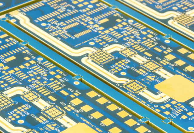
A Low Loss PCB is a printed circuit board designed using materials and structures that minimize signal attenuation (loss) during transmission, especially in high-frequency and high-speed applications.
As data rates and frequencies increase, signal loss becomes a critical issue. Standard PCB materials like FR4 introduce higher dielectric loss, making them unsuitable for advanced designs.
Low loss PCBs are specifically engineered to maintain signal integrity, reduce attenuation, and ensure reliable performance.
Why Signal Loss Matters
In high-speed and RF circuits, signal loss leads to:
- Reduced signal strength
- Increased bit error rates
- Poor impedance matching
- Degraded system performance
Key Parameters of Low Loss PCB
1. Dissipation Factor (Df)
The most critical parameter for loss:
- Lower Df = lower signal loss
- Typical low loss materials: Df < 0.005
2. Dielectric Constant (Dk) Stability
Stable Dk ensures consistent impedance and signal propagation.
3. Surface Roughness
Smoother copper reduces conductor loss at high frequencies.
4. Frequency Range
Loss increases with frequency, making material selection critical above 1 GHz.
Loss Mechanism (Simplified)
Total Loss=Dielectric Loss+Conductor Loss\text{Total Loss} = \text{Dielectric Loss} + \text{Conductor Loss}Total Loss=Dielectric Loss+Conductor Loss
Materials for Low Loss PCB
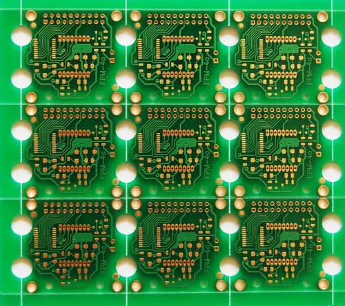
1. Modified FR4 (Mid-Loss)
- Improved over standard FR4
- Suitable for mid-speed applications
2. High-Speed Laminates
- Lower Df and stable Dk
- Used in networking and data centers
3. PTFE-Based Materials
- Ultra-low loss
- Ideal for RF and microwave
4. Advanced Hydrocarbon/Ceramic Materials
- Balance between performance and manufacturability
Low Loss PCB vs Standard PCB
| Feature | Low Loss PCB | Standard FR4 PCB |
|---|---|---|
| Signal Loss | Low | Higher |
| Frequency Support | High (>1 GHz) | Limited |
| Signal Integrity | Excellent | Moderate |
| Cost | Higher | Lower |
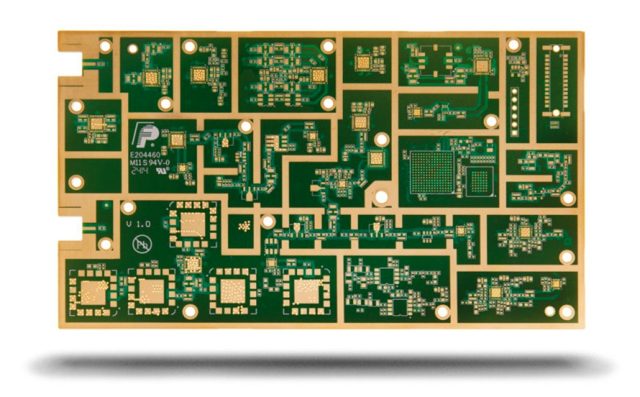
Applications of Low Loss PCB
1. High-Speed Digital Systems
Servers, switches, and data center hardware.
2. 5G Communication
Base stations and RF front-end modules.
3. RF & Microwave Circuits
Amplifiers, antennas, and filters.
4. Aerospace & Defense
Radar and satellite communication systems.
5. High-Performance Computing
AI servers and high-speed interconnects.
Design Considerations
1. Controlled Impedance
Accurate impedance design is essential to minimize reflection.
2. Short Signal Paths
Reduce insertion loss and delay.
3. Smooth Copper Selection
Use low-profile or ultra-low-profile copper.
4. Stack-Up Optimization
Layer structure directly impacts signal performance.
5. Minimize Vias
Reduce discontinuities in high-speed paths.
Manufacturing Challenges
Low Loss PCB requires strict process control:
- Tight impedance tolerance
- Consistent dielectric thickness
- Advanced material handling
- Precision etching
When Should You Choose Low Loss PCB?
Choose Low Loss PCB when:
- Data rates are high (e.g., >10 Gbps)
- Frequency exceeds 1 GHz
- Signal integrity is critical
- Long trace routing is required
Avoid it if:
- Low-speed applications
- Cost-sensitive designs
- No strict signal requirements
Conclusion
Low Loss PCB is essential for modern high-speed and high-frequency electronics, enabling reliable signal transmission and system stability.
By combining the right materials, proper design, and precise manufacturing, low loss PCBs ensure optimal performance in demanding applications.
