Why Loss Matters in Modern PCB Design
As data rates and frequencies continue to increase, signal loss becomes one of the primary limiting factors in PCB performance. In high-speed digital systems and RF designs, excessive loss leads to:
- Signal degradation and eye diagram closure
- Reduced transmission distance
- Increased bit error rates (BER)
- Lower system reliability
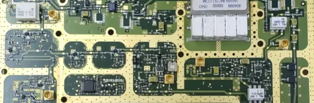
A Low Loss PCB is specifically designed to minimize signal attenuation, ensuring that signals maintain integrity over longer distances and at higher frequencies.
In applications such as data centers, 5G infrastructure, and high-speed computing, controlling loss is no longer optional—it is critical.
Where Does Signal Loss Come From?
Understanding loss mechanisms is essential for effective design.
- Dielectric Loss
Energy dissipates as heat within the PCB material. This is determined by the material’s dissipation factor (Df). - Conductor Loss
At high frequencies, current flows along the surface of copper (skin effect), increasing resistance and loss. - Surface Roughness Effects
Rough copper surfaces increase the effective path length of current, significantly increasing loss at high frequencies. - Radiation Loss
Poor routing or discontinuities can cause signals to radiate into the environment. - Via & Discontinuity Loss
Transitions such as vias and connectors introduce impedance mismatches and reflections.
In high-frequency systems, these losses combine to significantly impact overall performance.
Design Strategies to Reduce Loss
Reducing loss requires a combination of layout optimization and signal path control:
- Shorter Signal Paths:
Minimize trace length to reduce attenuation. - Controlled Impedance Routing:
Maintain consistent impedance to prevent reflections and additional loss. - Optimized Via Design:
Use back-drilling or microvias to eliminate via stubs. - Smooth Copper Selection:
Use low-profile or ultra-smooth copper foils to reduce conductor loss. - Proper Grounding:
Continuous reference planes improve return paths and reduce radiation loss. - Minimize Layer Transitions:
Each transition adds loss and potential impedance discontinuity.
These strategies are essential in maintaining high signal quality in multi-gigabit systems.
Material Selection Logic
Material choice is one of the most critical factors in achieving low loss performance.
Key material characteristics include:
- Low Dissipation Factor (Df):
Directly reduces dielectric loss, especially at high frequencies. - Stable Dielectric Constant (Dk):
Ensures consistent impedance and signal propagation. - Low Moisture Absorption:
Prevents performance degradation in varying environments. - Thermal Stability:
Maintains electrical properties across temperature changes.
Common low-loss material systems include:
- Modified FR-4 (mid-loss solutions)
- Hydrocarbon ceramic laminates
- PTFE-based materials (ultra-low loss)
- Advanced high-speed materials (e.g., Megtron series)
Often, designers use hybrid stack-ups to balance cost and performance.
When Do You Need a Low Loss PCB?
Low loss PCBs are essential when signal integrity becomes a limiting factor:
- High-speed digital interfaces (25G / 56G / 112G SerDes)
- 5G and mmWave communication systems
- High-frequency RF and microwave circuits
- Data center and networking equipment
- High-performance computing systems
If your design shows signs of signal attenuation, timing issues, or high BER, transitioning to a low loss PCB is often the most effective solution.
Final Thoughts
Low loss PCBs are not defined by a single material or feature—they are the result of careful engineering across materials, layout, and manufacturing processes.
As data rates continue to increase, minimizing loss becomes a core design priority, not just an optimization step.
By combining advanced materials, optimized routing strategies, and precise manufacturing control, KKPCB delivers Low Loss PCBs that support high-speed and high-frequency systems with reliable performance.
