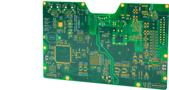
High-Density Interconnect (HDI) PCBs are a key technology for today’s compact and high-performance electronics. With fine lines, microvias, blind and buried vias, and multiple layers, HDI PCBs allow designers to fit complex circuits into small form factors, supporting applications from mobile devices to 5G infrastructure, automotive electronics, aerospace systems, and industrial IoT devices.
Advanced Design Strategies
-
Microvia Implementation:
HDI PCBs rely heavily on microvias, which are laser-drilled holes connecting adjacent layers. These microvias reduce signal path lengths, minimize parasitic inductance, and improve high-speed signal transmission. Designers often use stacked or staggered microvias to optimize routing density while maintaining electrical performance. -
Fine Line and Space Routing:
As device footprints shrink, trace widths and spacing must be reduced to tens of microns. Careful attention to etching tolerances and copper balance is required to prevent shorts, opens, or impedance variation, especially in high-frequency applications. -
Materials Selection:
HDI PCBs often use advanced substrates with low dielectric constants and low loss tangent to maintain signal integrity at high frequencies. Materials like FR-4 high-performance variants, Rogers laminates, and hybrid composites are chosen based on signal speed, thermal performance, and mechanical stability. -
Signal Integrity and Power Integrity:
High-speed digital circuits require controlled impedance, differential pair routing, and careful layer stackup design. Decoupling capacitors, power planes, and via placements are optimized to reduce noise, crosstalk, and voltage drop, ensuring consistent performance even in dense multilayer configurations.
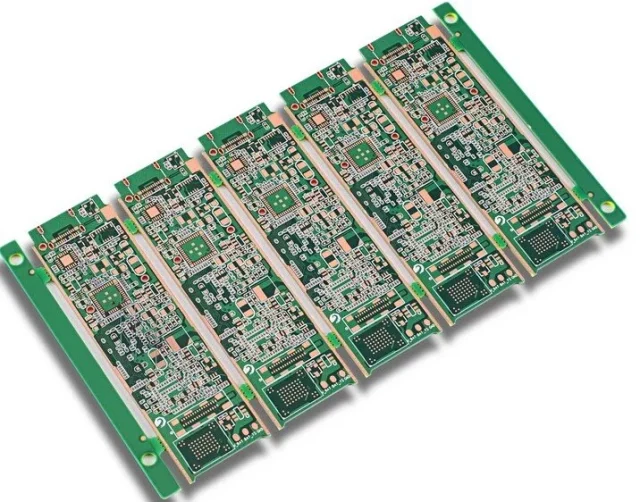
Manufacturing Considerations
Producing HDI PCBs requires advanced fabrication techniques and precise process control:
-
Sequential Lamination: Each HDI layer is laminated in stages to accommodate microvias and buried connections.
-
Laser Drilling: Microvias are formed with high-precision lasers to ensure minimal misalignment and reliable electrical connectivity.
-
Via Filling and Plating: Copper filling or plating in microvias enhances thermal dissipation and mechanical robustness, particularly for stacked via structures.
-
Panel and Board Handling: HDI PCBs are more delicate due to thin copper and dense traces, requiring careful handling and cleanroom conditions to prevent defects.
KKPCB leverages these advanced processes to maintain high yield and ensure performance for complex HDI projects.
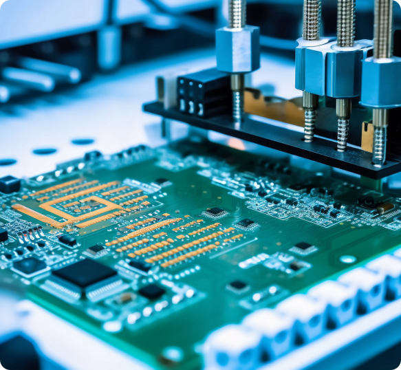
Testing and Quality Assurance
HDI PCBs demand rigorous inspection and testing due to their complexity:
-
Automated Optical Inspection (AOI): Detects surface defects and misalignments.
-
X-ray Inspection: Verifies internal microvias and buried structures.
-
Electrical Testing: Confirms continuity, impedance, and high-frequency signal paths.
-
Thermal and Reliability Testing: Ensures the PCB withstands operational heat, vibration, and environmental stress, critical for automotive, aerospace, and industrial applications.
Applications and Market Impact
HDI technology enables innovation across multiple industries:
-
Mobile Devices and Wearables: Ultra-compact designs with high pin counts and advanced functionality.
-
5G Infrastructure and Networking: High-speed signal transmission with minimal interference for next-generation communication.
-
Automotive Electronics and ADAS: Supporting sensor integration, compact control units, and robust reliability.
-
Aerospace and Defense: Multi-layer, high-density boards for avionics and mission-critical electronics.
-
Industrial IoT and Smart Devices: Dense, reliable PCBs for sensors, controllers, and embedded systems.
With HDI PCBs, engineers can push the boundaries of miniaturization, improve electrical performance, and create more robust devices. KKPCB’s expertise in HDI design, materials selection, precise fabrication, and thorough testing ensures that customers receive high-quality boards capable of meeting stringent modern electronics requirements.
