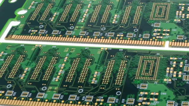
As electronic devices become smaller and more complex, the need for high-density interconnections within printed circuit boards increases. Buried via PCBs offer a solution by connecting inner layers without using surface space, allowing for compact, high-performance multilayer boards.
Buried vias improve routing flexibility, signal integrity, and design density, making them critical for advanced applications such as high-speed computing, telecommunications, and aerospace electronics.
What is a Buried Via PCB?
A Buried Via PCB is a multilayer printed circuit board where some vias (electrical connections between layers) are placed entirely within the inner layers, not extending to the top or bottom surface.
Types of vias in multilayer PCBs include:
-
Through-hole vias: Pass from top to bottom layers
-
Blind vias: Connect outer layers to inner layers but do not pass through the entire board
-
Buried vias: Connect only inner layers and are invisible on the surface
Buried vias allow for more complex routing and save surface space for components.
Advantages of Buried Via PCB
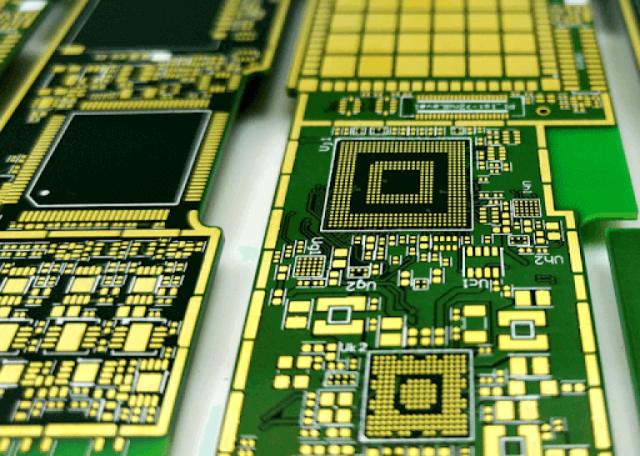
1. High-Density Interconnects
Buried vias enable more connections between inner layers without occupying surface area, allowing designers to increase component density on the PCB.
2. Improved Signal Integrity
By reducing via stubs and optimizing interlayer connections, buried vias help maintain clean high-speed signal transmission, making them ideal for high-speed and high-frequency applications.
3. Compact PCB Design
Buried vias free up space on outer layers, allowing designers to place more components on the surface and reduce board size.
4. Enhanced Reliability
Reducing the number of through-hole connections lowers mechanical stress and potential failure points, increasing overall PCB reliability.
Design Considerations
When designing buried via PCBs, engineers must consider:
-
Layer stack-up planning: Proper placement of inner layer connections
-
Via diameter and aspect ratio: Ensures reliable plating and signal performance
-
Controlled impedance routing: Especially for high-speed digital and RF signals
-
Thermal management: Proper heat dissipation for dense multilayer boards
Careful design ensures electrical performance and manufacturability.
Manufacturing Challenges
Buried via PCBs require advanced fabrication techniques:
-
Inner layers must be pre-drilled and plated before final lamination
-
Accurate alignment of inner layers is critical
-
Multilayer lamination processes must maintain via integrity
-
Quality testing ensures plated vias are continuous and defect-free
Experienced PCB manufacturers are essential to achieve reliable buried via PCBs.
Applications of Buried Via PCB
Buried via PCBs are widely used in applications requiring high-density interconnects and reliable performance:
-
High-speed computing systems (servers, CPUs, GPUs)
-
Telecommunication equipment (5G and networking devices)
-
Aerospace and defense electronics
-
Medical electronics (imaging and diagnostic devices)
-
Consumer electronics (smartphones, tablets, and compact devices)
Conclusion
Buried via PCBs provide a sophisticated solution for high-density, high-speed, and compact electronic designs. By connecting inner layers without consuming surface space, they enable smaller, faster, and more reliable circuits.
Advanced design strategies, careful material selection, and precise manufacturing make buried via PCBs a crucial technology for modern electronics innovation.
