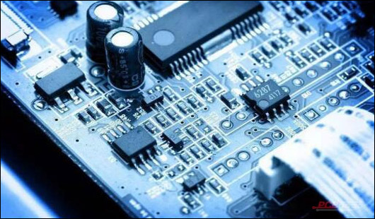
As electronic devices continue to operate at higher speeds, maintaining signal integrity becomes a critical design challenge. Variations in impedance along a signal path can cause reflection, signal loss, and timing issues, potentially compromising system performance.
Impedance controlled PCBs are specifically designed to maintain a consistent impedance across high-speed traces, ensuring reliable signal transmission in demanding applications. They are widely used in high-frequency RF circuits, data communication devices, and high-speed digital systems.
What is an Impedance Controlled PCB?
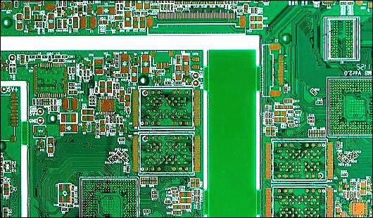
An impedance controlled PCB is a circuit board in which the designer carefully controls the width, thickness, and spacing of traces, as well as dielectric properties of the PCB materials, to achieve a target impedance for specific signal paths.
Key features include:
-
Consistent trace impedance for signal integrity
-
Optimized trace width and spacing based on PCB stack-up
-
Careful selection of dielectric materials for low loss and stability
-
Minimized signal reflections and crosstalk
Maintaining precise impedance is critical for high-speed and RF circuits where even small variations can affect performance.
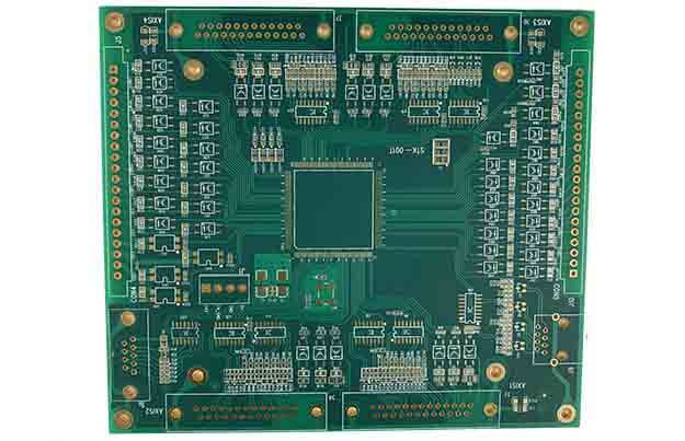
Key Applications of Impedance Controlled PCB
Impedance controlled PCBs are essential in any high-speed or high-frequency electronic system. Common applications include:
-
High-speed digital circuits (DDR memory, PCIe, USB, HDMI)
-
RF modules and communication devices
-
5G and wireless communication equipment
-
Networking switches, routers, and servers
-
High-speed sensor and measurement systems
-
Automotive electronics and radar systems
Design Principles of Impedance Controlled PCB
1. Controlled Trace Impedance
-
Trace width, thickness, and spacing are calculated to meet the required characteristic impedance (commonly 50Ω, 75Ω, or differential 100Ω).
-
Proper impedance ensures minimal signal reflection and maximum data integrity.
2. PCB Stack-Up Design
-
Multilayer stack-ups are optimized for signal routing, reference planes, and ground planes.
-
Ground and power planes are carefully placed to control return paths and reduce crosstalk.
3. Material Selection
-
Low-loss laminates such as Rogers, FR-4 high-frequency variants, or PTFE-based substrates are used depending on frequency requirements.
-
Stable dielectric constant (Dk) is critical for maintaining impedance consistency.
4. Differential Pair Routing
-
For high-speed serial signals, differential pair routing is implemented.
-
Matched trace lengths and spacing maintain the differential impedance, reducing noise and signal degradation.
5. Signal Integrity Optimization
-
Proper via placement, controlled transitions, and impedance-matched connectors are used to minimize reflection.
-
Termination techniques may also be applied to improve signal quality.
Manufacturing Considerations
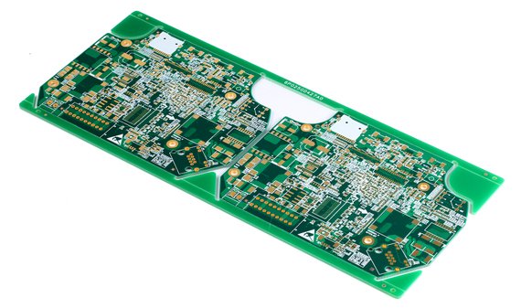
Producing impedance controlled PCBs requires high precision in both design and fabrication:
-
Tight tolerance on trace width, spacing, and copper thickness
-
Accurate dielectric material selection and layer thickness control
-
High-quality lamination and via drilling processes
-
Testing and validation for impedance consistency across production runs
Reliable manufacturing ensures that the PCB meets high-speed design requirements and maintains system performance.
Conclusion
Impedance controlled PCBs are a cornerstone of modern high-speed electronics. By maintaining consistent impedance along critical signal paths, these PCBs ensure signal integrity, reduced reflection, and reliable operation in high-frequency, high-speed, and RF applications.
Choosing the right materials, stack-up design, and manufacturing process is essential for delivering PCBs that meet the demanding performance requirements of networking devices, automotive electronics, and advanced computing systems.
