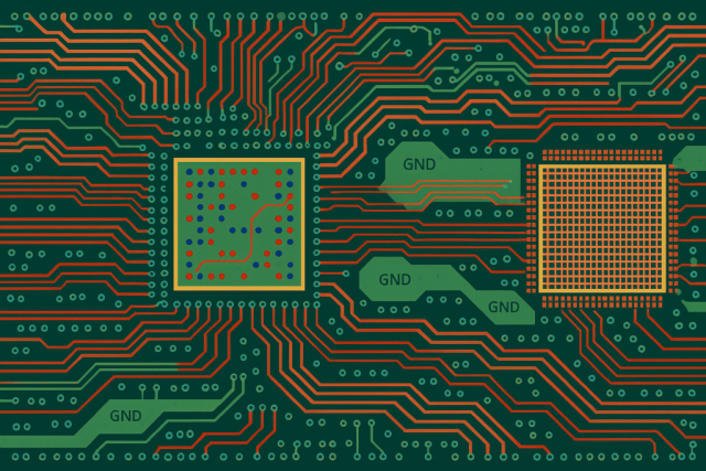
What Is a 5G mmWave PCB?

A 5G mmWave PCB is a specialized printed circuit board designed to handle millimeter-wave (mmWave) signals used in 5G wireless communication systems. Operating at extremely high frequencies, typically 24 GHz to 100 GHz, mmWave PCBs require precise impedance control, low dielectric loss, and high signal integrity to ensure efficient transmission and minimal signal attenuation.
These PCBs are crucial for 5G devices such as base stations, small cells, antennas, transceivers, and high-speed modules, where traditional PCB materials like FR4 cannot meet the performance demands of mmWave signals.
Key Properties of 5G mmWave PCBs
1. Low Dielectric Loss
5G mmWave PCBs use low-loss dielectric materials to reduce signal attenuation at high frequencies. Common materials include:
-
PTFE-based laminates
-
Rogers RO4350B or RO4003 series
-
Ceramic-filled hydrocarbon laminates
2. Precise Impedance Control
Maintaining consistent impedance is critical at mmWave frequencies to prevent signal reflection, distortion, and insertion loss. Designers carefully control:
-
Trace width and spacing
-
Dielectric thickness
-
Layer stack-up configuration
3. High-Frequency Performance
These PCBs support GHz-range signals with minimal interference, enabling high-speed data transmission for 5G networks. Proper design reduces crosstalk, insertion loss, and phase distortion.
4. Thermal Stability
High-frequency 5G circuits can generate significant heat. mmWave PCBs require materials with low thermal expansion and excellent thermal conductivity to ensure stable performance and prevent delamination or warping.
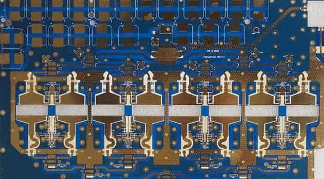
Design Considerations for 5G mmWave PCBs
Designing an effective mmWave PCB involves:
-
Layer Stack-Up Optimization – Balancing signal, power, and ground layers for minimal interference.
-
Controlled Impedance Routing – Maintaining exact trace width, spacing, and dielectric properties.
-
Minimizing Parasitics – Reducing vias, stubs, and sharp corners that can degrade signal integrity.
-
High-Precision Manufacturing – Advanced fabrication processes, including laser-drilled microvias and smooth copper plating, to support high-frequency performance.
These considerations ensure low-loss signal transmission and reliable operation for 5G devices.
Applications of 5G mmWave PCBs
5G mmWave PCBs are widely applied in next-generation communication systems:
-
5G base stations and small cell modules
-
mmWave antennas and beamforming arrays
-
High-speed transceivers and RFIC modules
-
5G IoT and consumer devices
-
Automotive radar systems
The increasing demand for high-frequency, high-bandwidth 5G networks makes mmWave PCBs essential for modern telecommunication infrastructures.
Advantages of Using 5G mmWave PCBs
-
High-Speed Data Transmission – Supports multi-GHz frequencies for fast 5G communication.
-
Signal Integrity – Low-loss materials and precise impedance control minimize distortion.
-
Compact Designs – Enables dense PCB layouts for small 5G modules and antennas.
-
Reliability in Harsh Environments – Thermal stability ensures consistent performance under high power and temperature variations.
-
Future-Proof Technology – Supports 5G and emerging 6G mmWave applications.
Conclusion
A 5G mmWave PCB is critical for high-frequency, high-bandwidth wireless systems. With low-loss materials, precise impedance control, and advanced fabrication techniques, these PCBs provide reliable signal transmission for 5G base stations, antennas, and high-speed transceivers. As 5G networks continue to expand globally, mmWave PCBs are key to achieving efficient, high-performance communication systems.
