What Is an mmWave Module PCB?
A mmWave Module PCB is a specialized printed circuit board engineered to support millimeter-wave frequencies, typically ranging from 24 GHz to 100 GHz.
Unlike standard RF or microwave PCBs, mmWave PCBs require:
-
Extremely low-loss materials
-
Precise impedance control
-
Ultra-compact and dense layouts
-
Minimal signal reflection and crosstalk
These PCBs are critical for applications that demand ultra-high-speed data transfer, precision radar sensing, and high-frequency wireless communication.
Key Design Considerations
1. Low-Loss Materials
At millimeter-wave frequencies, even small dielectric losses can drastically reduce signal strength.
Common material choices include:
-
PTFE-based laminates
-
Rogers RO4000 / RO4350B series
-
Taconic high-frequency laminates
Key material properties include low dielectric constant (Dk), low dissipation factor (Df), and thermal stability, ensuring predictable RF performance across operating conditions.
2. Controlled Impedance Routing
mmWave signals are highly sensitive to impedance mismatches. Design strategies include:
-
Microstrip and stripline structures
-
Precise trace width and spacing
-
Differential pair routing for high-speed signals
-
Via minimization or back-drilled vias to remove stubs
Proper controlled impedance maintains signal integrity and reduces reflection losses, critical for radar and 5G front-end modules.
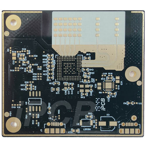
3. Multilayer and HDI Design
To support dense component placement and complex routing, mmWave Module PCBs typically feature:
-
4–12+ layer stack-ups
-
HDI (High-Density Interconnect) with microvias
-
Ground and power plane separation
-
Shielded RF layers
Multilayer HDI design enables compact module sizes while minimizing EMI and improving high-frequency signal isolation.
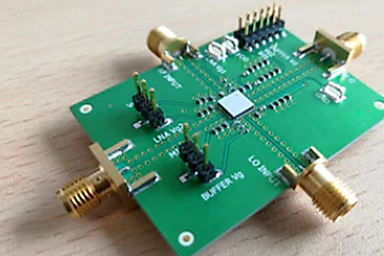
4. Antenna and RF Front-End Integration
mmWave modules often integrate:
-
Patch antennas or array antennas
-
Low-noise amplifiers (LNA)
-
Power amplifiers (PA)
-
Bandpass filters and matching networks
PCB layout must optimize signal paths, return currents, and shielding to maintain maximum radiation efficiency and minimal loss.
5. Thermal and Mechanical Stability
High-frequency mmWave chips can generate significant heat in a compact form factor. Effective thermal management includes:
-
Thermal vias under BGA packages
-
Heavy copper planes for heat spreading
-
Balanced layer stack to prevent warpage
-
Reinforced PCB structure for vibration resistance
Thermal stability ensures consistent RF performance over temperature fluctuations.
Applications of mmWave Module PCB
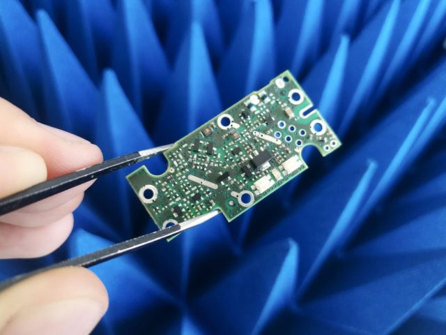
-
5G NR front-end modules and routers
-
Automotive radar (adaptive cruise control, collision avoidance)
-
Satellite communication and phased array antennas
-
High-speed wireless IoT devices
-
Industrial sensing and measurement systems
In all these applications, mmWave PCBs are critical for high-precision, high-speed signal transmission in compact modules.
mmWave PCB vs Standard RF PCB
| Feature | Standard RF PCB | mmWave Module PCB |
|---|---|---|
| Frequency Range | <6 GHz | 24–100 GHz |
| Material | FR4 or basic RF laminate | Low-loss PTFE / Rogers / Taconic |
| Impedance Control | Moderate | Critical |
| Signal Integrity | Moderate | Ultra-sensitive |
| Layer Density | 2–6 layers | 4–12+ layers HDI |
| Size | Moderate | Compact, module-scale |
mmWave Module PCBs are designed for extreme high-frequency performance, minimal loss, and dense integration, unlike conventional RF PCBs.
Conclusion
A mmWave Module PCB is a high-performance, high-frequency platform designed for 5G, automotive radar, satellite, and industrial sensing applications.
By combining low-loss materials, precise impedance routing, multilayer HDI design, and careful thermal management, mmWave PCBs ensure stable, high-speed signal transmission in compact, high-density modules.
They are essential for the next generation of wireless communication and sensing technologies.
