What Is a Blind Via PCB?
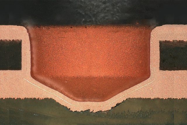
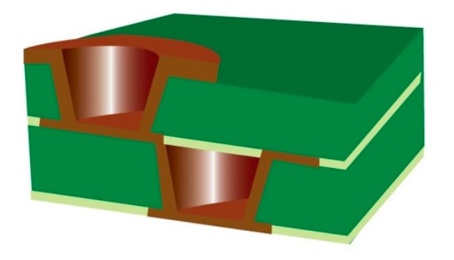
A Blind Via PCB is a type of multilayer printed circuit board where vias connect outer layers to one or more inner layers without passing completely through the board.Unlike through-hole vias, blind vias are partially embedded, allowing higher component density and more complex multilayer designs.
They are widely used in:
-
High-speed computing boards
-
RF and microwave modules
-
Mobile devices and IoT modules
-
Aerospace and automotive electronics
Blind vias are essential for miniaturized electronics and high-density interconnect (HDI) designs.
Key Advantages of Blind Via PCB
1. Higher Component Density
Blind vias free up surface area by:
-
Avoiding full board penetration
-
Allowing smaller via pads on outer layers
-
Supporting more routing space for fine-pitch components
This enables designers to pack more functionality in smaller form factors, which is crucial in mobile devices and compact electronics.
2. Improved Signal Integrity
In high-frequency and high-speed circuits, blind vias offer:
-
Reduced via stub length
-
Minimized reflection and signal loss
-
Lower crosstalk between traces
Shorter stubs and controlled impedance help maintain signal quality in GHz-level RF and digital circuits.
3. Enhanced Multilayer Flexibility
Blind vias allow complex multilayer stack-ups:
-
Outer layers routed independently
-
Inner layers connected selectively
-
Power and ground planes optimized
This flexibility is particularly important for HDI PCBs, 5G modules, and high-speed data boards.
4. Better Thermal and Mechanical Performance
By limiting the via to required layers, blind vias:
-
Reduce stress on the PCB structure
-
Help prevent delamination during thermal cycling
-
Maintain dimensional stability
This ensures reliable operation under automotive, aerospace, and industrial conditions.
Manufacturing Considerations
Producing blind via PCBs requires precise fabrication processes:
-
Laser or mechanical drilling for partial-layer vias
-
Controlled via plating thickness
-
Fine registration alignment for multilayer lamination
-
High-TG and low-loss materials to maintain electrical performance
Proper manufacturing ensures high yield, consistent impedance, and minimal signal degradation.
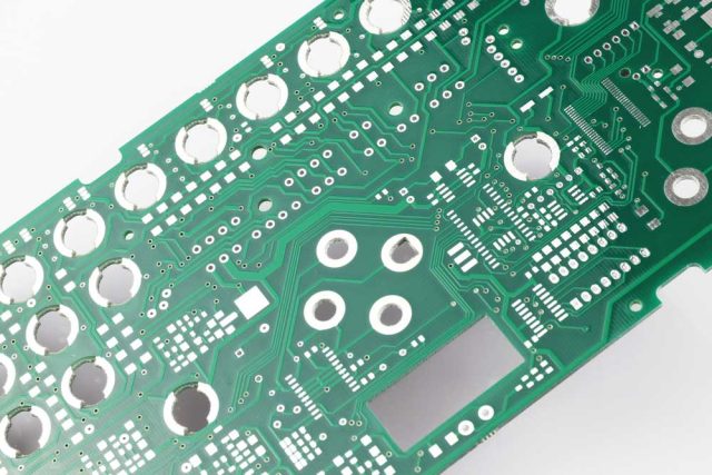
Applications of Blind Via PCB
Blind via PCBs are commonly used in:
-
5G communication modules
-
High-frequency RF front-end circuits
-
Smartphones and compact electronics
-
Automotive radar and sensor boards
-
Aerospace electronics with weight and space constraints
In these applications, blind vias enable compact, reliable, and high-performance PCB layouts.
Blind Via PCB vs Through-Hole PCB
| Feature | Through-Hole PCB | Blind Via PCB |
|---|---|---|
| Layer Connection | Outer-to-outer and inner-to-inner | Outer-to-inner (partial) |
| Component Density | Moderate | High |
| Signal Integrity | Moderate | Excellent for high-speed |
| Board Thickness | Limited by via | Flexible for HDI |
| Manufacturing Complexity | Simple | Higher |
Blind vias are indispensable for modern high-speed and high-density electronics.
Conclusion
A Blind Via PCB is a high-density, high-performance solution for multilayer electronic designs.By connecting outer layers to selected inner layers, blind vias allow compact layouts, improved signal integrity, and flexible multilayer stack-ups.
They are ideal for applications ranging from 5G modules and RF circuits to automotive and aerospace electronics, where miniaturization and high-speed performance are critical.
