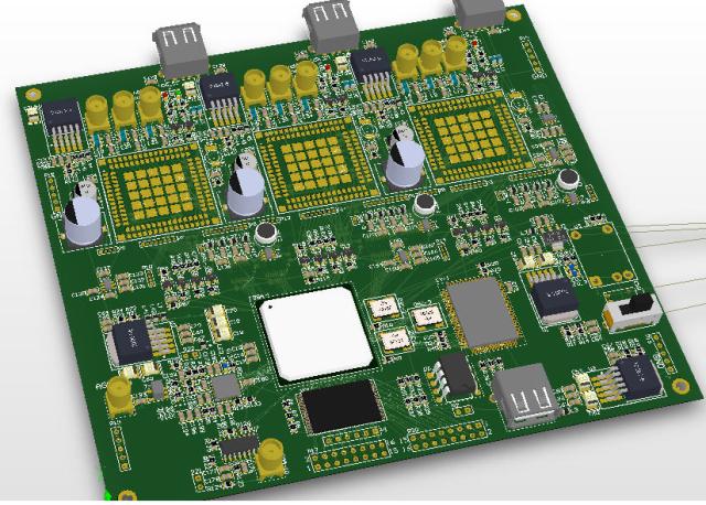
What Is a 5G IC Test PCB?

A 5G IC Test PCB is a specialized printed circuit board designed for functional testing, RF validation, and high-speed performance verification of 5G integrated circuits.
Unlike standard application PCBs, test PCBs are engineered to provide stable signal paths, accurate impedance control, and minimal insertion loss during chip evaluation and production testing.
They are commonly used during:
-
Engineering validation testing (EVT)
-
Design verification testing (DVT)
-
Production testing
-
RF characterization
-
High-speed interface validation
Why 5G IC Testing Requires Advanced PCB Design
5G chips operate at high frequencies, often in sub-6GHz and mmWave bands. At these frequencies, PCB performance directly impacts test accuracy.
Key challenges include:
-
RF signal attenuation
-
Impedance mismatch
-
Signal reflection
-
Crosstalk
-
Parasitic effects
-
Phase instability
A properly designed 5G IC test PCB ensures reliable and repeatable measurement results.
Key Design Features
1. Controlled Impedance Routing
Precise 50Ω single-ended and 100Ω differential impedance structures are required for:
-
RF signal lines
-
High-speed SERDES
-
Clock routing
Stack-up design must be carefully calculated to maintain consistency.
2. Low-Loss Substrate Materials
To reduce insertion loss at high frequencies, test PCBs often use advanced materials such as:
-
Low-loss RF laminates
-
PTFE-based materials
-
Hydrocarbon ceramic-filled substrates
Material selection directly affects measurement accuracy.
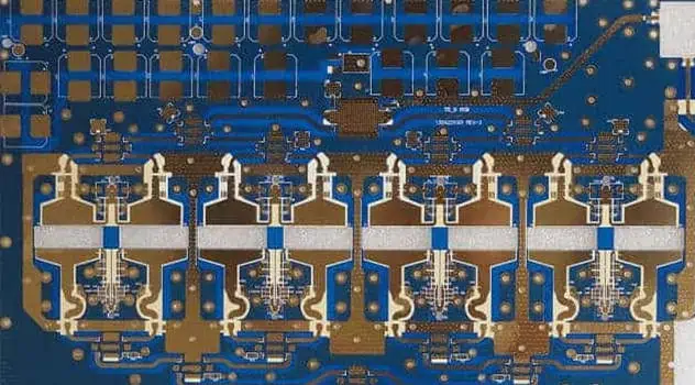
3. RF Connector and Launch Design
High-frequency connectors (SMA, SMP, etc.) must be properly matched to PCB traces to avoid reflection and loss.
Transition design between connector and microstrip/stripline structure is critical.
4. Fine Pitch and BGA Escape Routing
5G ICs typically use:
-
Fine pitch BGA packages
-
High pin count configurations
HDI structures and microvias are often required to support routing density.
5. Thermal Management
During RF testing and burn-in processes, chips may generate significant heat. Thermal vias and copper planes are integrated to maintain stable operating conditions.
Applications of 5G IC Test PCB
5G IC test boards are widely used in:
-
RF transceiver chip validation
-
mmWave front-end module testing
-
Baseband processor evaluation
-
Power amplifier testing
-
Production ATE environments
-
IoT 5G module development
Accurate PCB design ensures repeatable and trustworthy test results.
5G IC Test PCB vs Standard 5G PCB
| Feature | Standard 5G PCB | 5G IC Test PCB |
|---|---|---|
| Purpose | Product application | Chip validation & testing |
| Design Focus | Function integration | Signal accuracy & stability |
| Material | Performance-based | Measurement-optimized |
| Connector Integration | Optional | Critical |
| Repeatability | Moderate | High |
Test PCBs prioritize electrical precision over cost optimization.
Conclusion
A 5G IC Test PCB plays a critical role in validating the performance and reliability of high-frequency integrated circuits. Through controlled impedance design, low-loss materials, precise RF transitions, and stable stack-up engineering, it ensures accurate testing and consistent production results.
As 5G and mmWave technologies continue to advance, high-quality test PCB platforms remain essential for successful chip development and manufacturing.
