What Is a Multilayer PCB?
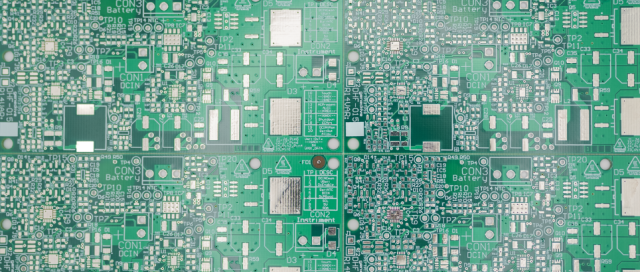
A Multilayer PCB is a printed circuit board consisting of three or more conductive copper layers laminated together with insulating dielectric materials. These layers are electrically interconnected through plated vias to create complex routing structures within a compact footprint.
Compared to single-layer or double-layer boards, multilayer PCBs enable higher circuit density, improved signal integrity, and greater design flexibility.
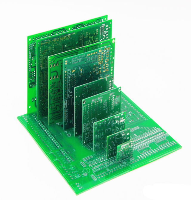
Basic Structure of a Multilayer PCB
A typical multilayer PCB stack-up includes:
-
Signal layers
-
Power planes
-
Ground planes
-
Prepreg bonding layers
-
Core materials
Copper layers are pressed together through controlled lamination processes to ensure structural integrity and electrical reliability.
Common configurations include:
-
4-layer PCB
-
6-layer PCB
-
8-layer PCB
-
10+ layer high-density designs
-
High layer count (20+ layers) systems
The number of layers depends on signal complexity and routing requirements.
Why Choose a Multilayer PCB?
As electronic systems grow more complex, multilayer structures provide significant advantages:
1. Higher Routing Density
Multiple signal layers allow compact designs without increasing board size.
2. Improved Signal Integrity
Dedicated ground and power planes reduce noise and electromagnetic interference.
3. Better Impedance Control
Controlled stack-up design ensures stable impedance for high-speed signals.
4. Reduced EMI
Internal plane layers act as shielding, improving electromagnetic compatibility.
Design Considerations
Designing a multilayer PCB requires careful planning:
-
Stack-up symmetry
-
Layer sequence optimization
-
Impedance calculation
-
Crosstalk reduction
-
Thermal management
-
Via structure selection
Improper stack-up design can lead to signal reflection, warpage, and manufacturing challenges.
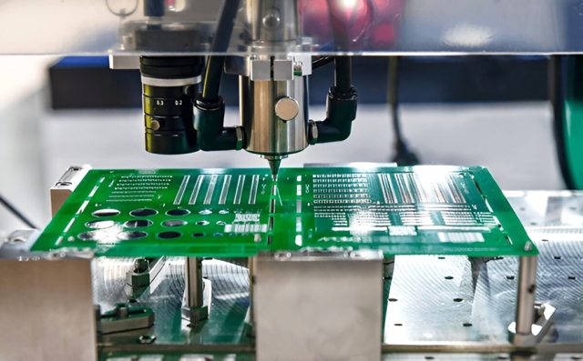
Manufacturing Process
Multilayer PCB fabrication involves:
-
Inner layer imaging and etching
-
Lamination under heat and pressure
-
Precision drilling
-
Via plating
-
Surface finishing
-
Electrical testing
Advanced boards may require sequential lamination and high aspect ratio drilling.
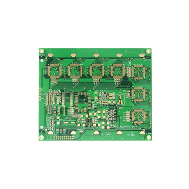
Applications of Multilayer PCB
Multilayer PCBs are widely used in:
-
High-speed computing systems
-
Data center networking equipment
-
5G communication devices
-
Automotive ADAS modules
-
Industrial control systems
-
Medical electronics
-
Aerospace systems
-
Consumer electronics
As performance requirements increase, multilayer structures become essential.
Multilayer PCB vs Double Layer PCB
| Feature | Double Layer PCB | Multilayer PCB |
|---|---|---|
| Layer Count | 2 | 3 or more |
| Routing Density | Limited | High |
| Signal Integrity | Moderate | Improved |
| EMI Control | Limited | Better |
| Complexity Support | Basic | Advanced |
Multilayer PCBs support complex, high-performance systems in compact form factors.
Conclusion
Multilayer PCB technology is fundamental to modern electronics. By integrating multiple conductive layers within a single structure, it enables compact design, improved signal performance, and higher functional integration.
For advanced communication, computing, automotive, and industrial systems, multilayer PCB remains a core platform for reliable and scalable electronic design.
