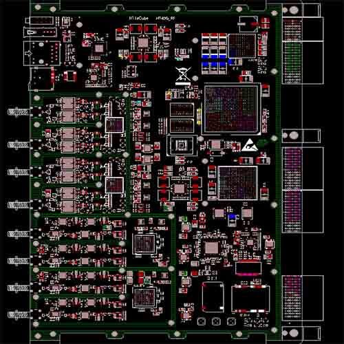
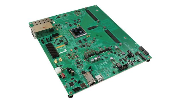
What Is a 5G mmWave PCB?

A 5G mmWave PCB is a high frequency printed circuit board engineered to operate at millimeter wave frequencies (typically 24 GHz to 100 GHz and above). These PCBs are used in advanced 5G communication systems where ultra-high bandwidth, low latency, and high data throughput are required.
At mmWave frequencies, signal loss, dielectric stability, and manufacturing precision become critical factors. Therefore, 5G mmWave PCB design requires specialized materials and tight process control.
Key Requirements of 5G mmWave PCB
1. Ultra-Low Loss Materials
To minimize signal attenuation at high frequencies, 5G mmWave PCB typically uses:
-
PTFE-based laminates
-
Hydrocarbon ceramic materials
-
Low Dk and low Df materials
-
Hybrid stack-ups combining RF core with high TG layers
Low dielectric loss ensures stable transmission across long RF traces.
2. Precise Impedance Control
At mmWave frequencies, even small impedance deviations can cause significant reflection and insertion loss.
5G mmWave PCB supports:
-
50Ω single-ended transmission lines
-
Differential pair routing
-
Microstrip and stripline structures
-
Tight impedance tolerance (±5% or better)
Accurate stack-up calculation and test coupon verification are essential.
3. High Frequency Design Optimization
Design considerations include:
-
Short RF trace routing
-
Via stub reduction (back drilling)
-
Grounded coplanar waveguide structures
-
Minimal discontinuities
-
Controlled surface roughness
Reducing conductor and dielectric loss is critical at mmWave bands.
4. Advanced Manufacturing Precision
5G mmWave PCB fabrication may include:
-
Fine line processing
-
Laser drilled microvias
-
Sequential lamination
-
High layer count RF stack-up
-
Strict dielectric thickness control
Manufacturing tolerances directly affect signal integrity and antenna performance.
Applications of 5G mmWave PCB
5G mmWave PCB is widely used in:
-
5G base station antenna modules
-
Phased array radar systems
-
RF front-end modules
-
Satellite communication systems
-
Automotive radar (77 GHz)
-
Wireless backhaul systems
-
High frequency IoT gateways
As global 5G deployment expands, mmWave PCB demand continues to grow.
Challenges in 5G mmWave PCB Design
Compared with standard RF PCB, 5G mmWave PCB faces:
-
Higher insertion loss sensitivity
-
Tighter impedance tolerance
-
Thermal management challenges
-
Increased material cost
-
Strict design-to-manufacturing coordination
Close collaboration between PCB manufacturer and RF design engineers is essential.
Why Choose a Professional 5G mmWave PCB Manufacturer
A reliable 5G mmWave PCB supplier should provide:
-
Experience with RF and microwave laminates
-
Precise impedance modeling and validation
-
Advanced drilling and lamination capability
-
Material traceability
-
Electrical testing and quality assurance
Professional manufacturing ensures stable performance at extremely high frequencies.
Conclusion
5G mmWave PCB is a critical component for next-generation wireless communication systems. With ultra-low loss materials, precise impedance control, and high precision fabrication, it enables stable operation at millimeter wave frequencies.
As 5G networks evolve toward higher bandwidth and faster speeds, selecting an experienced 5G mmWave PCB manufacturer is essential for achieving reliable and high performance RF systems.
