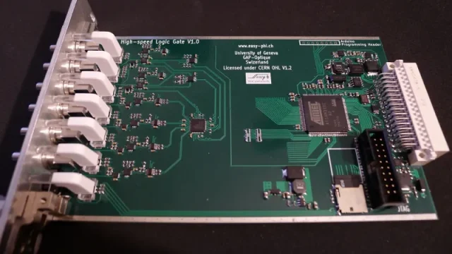
What Is a High Speed Logic PCB?
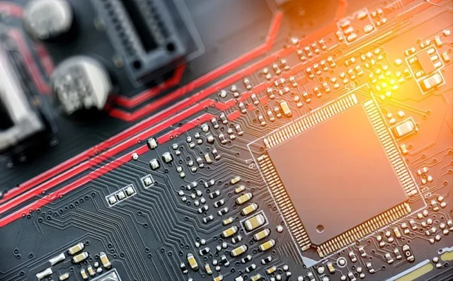
A High Speed Logic PCB is a printed circuit board designed to support high-speed digital logic circuits, where signal rise times are extremely fast and timing accuracy is critical. These PCBs ensure minimal signal distortion, precise timing, and reliable data transmission for high-performance computing, telecommunication, and semiconductor testing applications.
Why High Speed Logic PCB Technology Matters
Modern digital systems operate at gigahertz-level frequencies and require PCBs capable of maintaining signal integrity. Challenges addressed by high speed logic PCBs include:
-
Signal reflections due to impedance mismatch
-
Crosstalk between adjacent traces
-
Timing skew between differential pairs
-
Ground bounce and power noise
-
Signal attenuation over long or dense traces
Proper design and materials ensure stable operation and reliable logic performance.
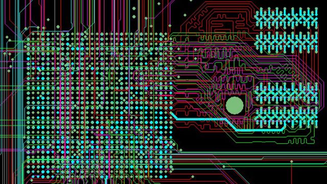
Key Features of High Speed Logic PCBs
High-quality high speed logic PCBs typically include:
-
Controlled impedance traces for matched signal paths
-
Optimized layer stackup for ground and power return paths
-
Low-loss dielectric materials to preserve signal quality
-
Short and matched trace routing for high-speed nets
-
Shielding and isolation for sensitive digital signals
These features are essential for high-frequency digital logic circuits and high-speed interfaces.
Design Considerations for High Speed Logic PCBs
Effective high speed logic PCB design requires:
-
Trace length matching for buses, DDR, PCIe, USB, or Ethernet
-
Differential pair routing for high-speed signals
-
Minimization of vias to reduce signal reflections
-
Crosstalk mitigation through spacing, ground shielding, and layer assignment
-
Layer stackup optimization for impedance and return paths
Design accuracy is critical to prevent timing errors and signal degradation.
Materials for High Speed Logic PCBs
Material selection affects both speed and reliability:
-
Low loss laminates for gigahertz-level signals
-
High TG FR-4 for thermal stability in dense boards
-
Hybrid materials for mixed-signal integration
-
Smooth copper foils to reduce insertion loss
-
Advanced laminates for high-frequency digital applications
Right materials ensure consistent signal propagation and reduced jitter.
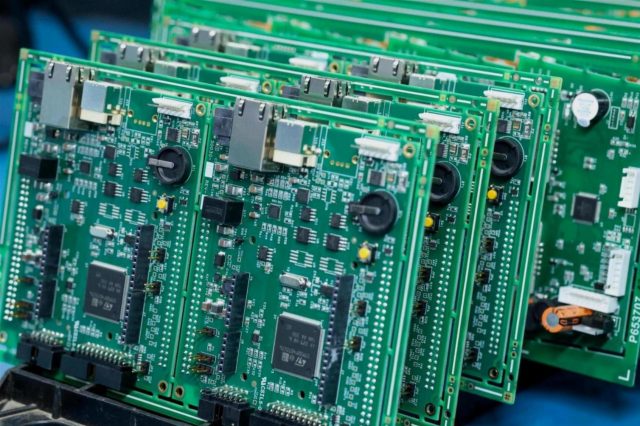
Manufacturing Capabilities for High Speed Logic PCBs
High speed logic PCB fabrication requires:
-
Precise etching for fine trace widths and spacing
-
Tight layer-to-layer registration
-
Controlled impedance verification (TDR testing)
-
Multilayer lamination and HDI capability
-
Automated inspection (AOI) and electrical testing
Advanced manufacturing ensures high-speed performance and signal integrity.
Assembly Considerations for High Speed Logic PCBs
Assembly for high speed logic PCBs includes:
-
Fine-pitch IC placement with precise soldering
-
Differential pair preservation during reflow
-
Controlled thermal profiles for sensitive components
-
Functional testing for high-speed signal operation
-
Shielding and connector integration for noise reduction
Proper assembly is crucial for maintaining logic speed and reliability.
Applications of High Speed Logic PCBs
High speed logic PCBs are widely used in:
-
High-performance computing (HPC) and servers
-
Networking and telecommunication equipment
-
High-speed ADC/DAC and data acquisition boards
-
5G and next-generation communication modules
-
Semiconductor test boards and ATE systems
-
Automotive ADAS and industrial automation
They are essential wherever fast, accurate digital signal transmission is required.
Why Choose a Professional High Speed Logic PCB Manufacturer
A professional manufacturer provides:
-
Expertise in high-speed digital PCB design
-
Stable manufacturing for controlled impedance and signal integrity
-
Support for prototypes, small batch, and mass production
-
Advanced inspection and electrical testing
-
One-stop PCB fabrication and assembly services
The right partner ensures high-speed performance, timing accuracy, and long-term reliability.
