What Is a Microvia PCB?
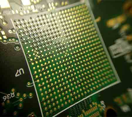
A Microvia PCB is a printed circuit board that uses microvias, which are very small drilled holes (typically <150 μm) to interconnect layers in high-density, multilayer HDI PCBs. Microvias enable fine-pitch routing, high pin count IC integration, and compact board layouts, making them essential for advanced electronics such as smartphones, 5G modules, semiconductor test boards, and aerospace systems.
Why Microvia PCB Technology Matters
As electronic devices continue to shrink and IC packages become more complex, traditional through-hole or standard via technology cannot meet density and performance requirements. Microvia PCBs provide solutions to challenges such as:
-
High-density component placement
-
Shorter signal paths for high-speed signals
-
Reduced parasitic capacitance and inductance
-
Controlled impedance for high-frequency applications
-
Efficient multilayer fan-out for fine-pitch ICs
They are especially crucial for HDI, RF, high-speed, and semiconductor test applications.
Key Features of Microvia PCBs
High-quality microvia PCBs typically offer:
-
Laser-drilled microvias for precise inter-layer connections
-
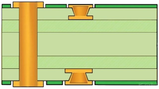
Blind and buried via integration for layer optimization
-
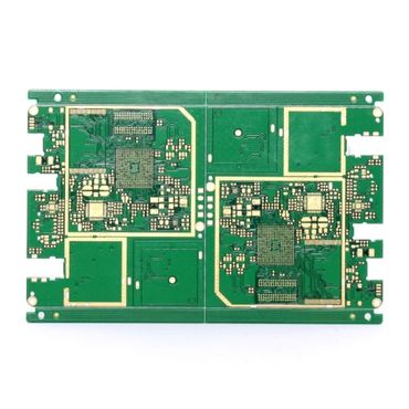
High layer count capability (8–30+ layers)
-
Controlled impedance and signal integrity
-
Support for fine-pitch BGA, QFN, and CSP packages
These features ensure high-density routing with minimal signal degradation.
Design Considerations for Microvia PCBs
Designing microvia PCBs requires close attention to:
-
Microvia diameter, aspect ratio, and plating thickness
-
Layer stackup optimization for impedance control
-
Short, matched signal paths for high-speed performance
-
Thermal management and via-in-pad strategies
-
Crosstalk and EMI mitigation
Proper design ensures both manufacturability and reliable electrical performance.
Materials for Microvia PCBs
Material selection is critical for microvia PCB performance:
-
High-Tg FR-4 for general HDI applications
-
Low-loss laminates for RF and high-speed signals
-
Polyimide materials for flexible HDI or rigid-flex designs
-
Advanced substrates for aerospace, 5G, and automotive use
Selecting the right material maintains signal integrity and ensures long-term reliability.
Manufacturing Capabilities for Microvia PCBs
Producing high-quality microvia PCBs requires:
-
Precision laser drilling and via formation
-
High layer-to-layer registration accuracy
-
Advanced lamination processes
-
Strict impedance control and verification
-
Automated optical inspection (AOI) and electrical testing
Professional manufacturing ensures consistent microvia quality and PCB reliability.
Assembly Considerations for Microvia PCBs
Microvia PCB assembly often involves:
-
Fine-pitch BGA/CSP placement and soldering
-
Controlled reflow and thermal profiles
-
High-accuracy solder paste printing
-
X-ray inspection for hidden microvia connections
-
ESD-safe handling and quality verification
Assembly quality is critical to fully leverage microvia PCB performance.
Applications of Microvia PCBs
Microvia PCBs are widely used in:
-
HDI smartphone and tablet motherboards
-
5G communication modules
-
High-speed networking and data center equipment
-
Semiconductor test boards and ATE systems
-
Automotive electronics and ADAS systems
-
Aerospace, satellite, and defense electronics
They enable compact, high-performance designs across industries.
Why Choose a Professional Microvia PCB Manufacturer
An experienced microvia PCB manufacturer provides:
-
Expertise in HDI and fine-pitch design
-
Stable quality for high layer count PCBs
-
Support for prototypes, small batches, and mass production
-
Advanced inspection and testing capabilities
-
One-stop PCB fabrication and assembly services
The right partner ensures high reliability, signal integrity, and successful integration of dense IC packages.
