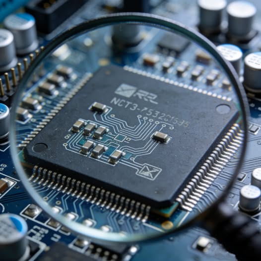
Low loss materials play a foundational role in modern PCB design where high-frequency, high-speed, and high-data-rate signals define system performance limits. As signal frequencies extend into multi-gigahertz and mmWave ranges, dielectric loss becomes a dominant factor affecting insertion loss, phase stability, and overall signal integrity. Selecting appropriate low loss materials is therefore a critical engineering decision rather than a simple material substitution.
Electrical Characteristics of Low Loss Materials
The defining feature of low loss materials is a low dissipation factor (Df), which minimizes dielectric energy loss as electromagnetic waves propagate through the substrate. In addition, low loss materials exhibit a stable dielectric constant (Dk) over frequency and temperature, ensuring predictable impedance behavior.
Key electrical advantages of low loss materials include:
-
Reduced insertion loss in high-frequency transmission lines
-
Improved eye diagram opening in high-speed digital links
-
Enhanced phase consistency for RF and microwave circuits
-
Tighter controlled impedance tolerance
These characteristics are essential for applications operating above several gigahertz, where conventional FR-4 materials introduce excessive signal attenuation.
Impact on Signal Integrity and Impedance Control
Signal integrity degradation at high frequencies often originates from dielectric variability rather than conductor loss alone. Low loss materials provide a more uniform electromagnetic environment, enabling precise impedance control in microstrip, stripline, and coplanar waveguide structures.
By using low loss materials, PCB designers can:
-
Minimize impedance discontinuities
-
Reduce signal reflections and return loss
-
Lower crosstalk in dense routing environments
-
Maintain consistent performance across temperature variations
This makes low loss materials a key enabler for high-speed digital and RF PCB architectures.
Thermal and Mechanical Stability Considerations
Beyond electrical performance, low loss materials must also provide sufficient thermal and mechanical stability to support complex multilayer PCB designs. Many advanced low loss laminates are engineered with high glass transition temperatures (Tg) and controlled coefficients of thermal expansion (CTE).
Thermal and mechanical benefits include:
-
Improved reliability during lead-free reflow assembly
-
Reduced warpage in high-layer-count PCBs
-
Stable via integrity under thermal cycling
-
Enhanced long-term mechanical durability
These properties are critical for maintaining signal integrity throughout the product lifecycle.
Manufacturing Considerations for Low Loss Materials
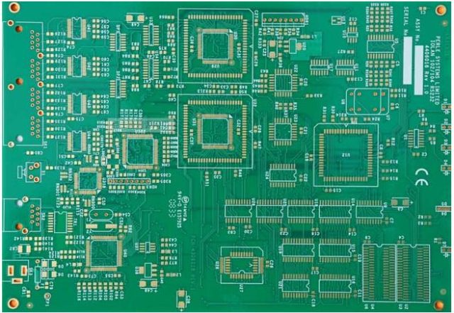
Fabrication of PCBs using low loss materials requires tighter process control compared to standard FR-4. Differences in resin chemistry and filler systems influence drilling behavior, copper adhesion, and lamination parameters.
Key manufacturing controls include:
-
Precision drilling and via formation
-
Controlled lamination temperature and pressure
-
Accurate etching for fine-line signal traces
-
Post-fabrication impedance verification
Consistent manufacturing processes are essential to fully realize the electrical advantages of low loss materials.
Application Domains
Low loss materials are widely adopted in:
-
High-speed digital backplanes and servers
-
RF and microwave communication systems
-
5G and mmWave wireless infrastructure
-
Satellite and aerospace electronics
-
High-performance test and measurement equipment
In these systems, low loss materials directly support higher bandwidth, lower bit error rates, and improved system reliability.
Engineering Perspective
Low loss materials are not an incremental upgrade—they are a fundamental requirement for modern high-frequency and high-speed PCB design. By reducing dielectric loss, stabilizing impedance, and supporting reliable manufacturing, low loss materials enable predictable signal behavior and scalable system performance.
Through disciplined material selection and process control, KKPCB supports engineers in implementing low loss material solutions optimized for advanced RF and high-speed digital applications.
