A High Frequency Signal PCB is a specialized printed circuit board engineered to transmit high frequency signals with low loss, stable impedance, and excellent signal integrity. As wireless communication and high-speed electronics continue to advance, high frequency PCB performance becomes a key factor in system stability, compliance, and overall product reliability.
Unlike standard PCBs used for low-speed digital circuits, a High Frequency Signal PCB must control transmission line behavior at MHz-to-GHz frequencies. At high frequency, signal energy is more sensitive to trace geometry, dielectric properties, copper roughness, and stack-up design. That is why High Frequency Signal PCB design requires strict control of controlled impedance, insertion loss, return loss, crosstalk, and EMI.
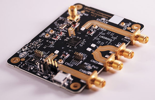
High Frequency Signal PCBs are widely used in RF communication, microwave systems, 5G modules, radar, GPS, WiFi, IoT devices, and high-speed digital systems that include sensitive RF paths.
What Is a High Frequency Signal PCB?
A High Frequency Signal PCB refers to a PCB designed for signal transmission at high frequency ranges, typically from hundreds of MHz up to multiple GHz. At these frequencies, PCB traces behave as transmission lines rather than simple interconnect wires.
To ensure stable high frequency signal performance, High Frequency Signal PCB designs commonly use:
-
Controlled impedance routing
-
Low loss PCB materials
-
Optimized multilayer stack-up
-
Stable ground reference planes
-
RF-friendly via structures and transitions
The goal of a High Frequency Signal PCB is to maintain consistent signal propagation while minimizing distortion, attenuation, and interference.
Why High Frequency Signal PCB Design Is Critical
High frequency signals are extremely sensitive to PCB design and manufacturing variation. Even small deviations in trace width, dielectric thickness, or copper surface quality can cause impedance mismatch and performance degradation.
Without proper High Frequency Signal PCB design, systems may face:
-
Higher insertion loss and signal attenuation
-
Reflection caused by impedance discontinuities
-
Increased jitter and reduced signal margin
-
Crosstalk and coupling between high frequency traces
-
EMI radiation and compliance failures
-
Unstable performance across temperature and environment
For modern RF and high-speed systems, High Frequency Signal PCB design is essential to achieve stable and repeatable results.
Key Features of High Frequency Signal PCB
1. Controlled Impedance for High Frequency Traces
Controlled impedance is the foundation of High Frequency Signal PCB performance. Common impedance requirements include:
-
50Ω single-ended impedance (RF signal routing)
-
75Ω impedance (video and certain RF systems)
-
90Ω / 100Ω differential impedance (high-speed digital links)
Controlled impedance depends on:
-
Trace width and spacing
-
Dielectric thickness
-
Copper thickness
-
Material dielectric constant (Dk)
-
Reference plane structure
Accurate impedance control reduces reflection and ensures stable high frequency signal transmission.
2. Low Loss PCB Materials for High Frequency Performance
Material selection is one of the most important decisions in High Frequency Signal PCB design. At high frequency, dielectric loss becomes significant, so low-loss materials help maintain signal strength.
Common High Frequency Signal PCB materials include:
-
Rogers PCB materials (RO4003C, RO4350B, RO3003)
-
PTFE / Duroid PCB materials for microwave designs
-
Megtron PCB / Megtron 6 PCB for ultra-low loss high-speed systems
-
High-performance FR-4 (for moderate frequency applications)
Low loss materials reduce attenuation and improve signal integrity across the frequency band.
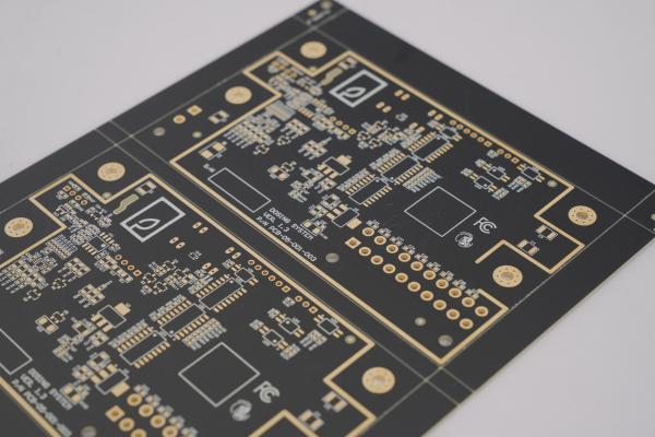
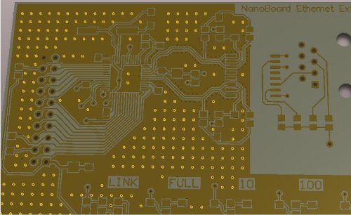
3. Optimized Stack-Up for High Frequency Signal Routing
A professional High Frequency Signal PCB requires stack-up planning to maintain stable impedance and return paths. Common routing structures include:
-
Microstrip traces (outer layer routing)
-
Stripline traces (inner layer routing)
-
Coplanar waveguide (CPW)
-
Grounded coplanar waveguide (GCPW)
Stack-up design helps improve:
-
Impedance stability
-
EMI shielding
-
Crosstalk control
-
High frequency signal isolation
A well-designed stack-up ensures stable high frequency performance in multilayer PCB designs.
4. Grounding and Return Path Control
High frequency signals require clean and continuous return paths. A High Frequency Signal PCB typically includes:
-
Solid ground planes under high frequency traces
-
Via stitching for stable grounding
-
Ground fences for shielding and isolation
-
Short return current paths to reduce loop area
Proper grounding improves signal integrity and reduces EMI radiation.
5. Via and Transition Optimization
Vias create impedance discontinuities at high frequency. High Frequency Signal PCB design must control via transitions through:
-
Minimizing via stubs
-
Reducing unnecessary layer transitions
-
Optimizing pad and anti-pad sizes
-
Using backdrill when required
-
Ensuring reference plane continuity
Optimized via structures help reduce reflection and improve insertion loss performance.
High Frequency Signal PCB Applications
High Frequency Signal PCBs are widely used in industries requiring stable RF and high frequency performance, including:
-
5G communication modules and base station systems
-
WiFi / Bluetooth wireless products
-
GPS navigation and positioning systems
-
Radar systems and automotive ADAS
-
Satellite and microwave communication equipment
-
IoT wireless sensor modules
-
RF front-end modules (FEM)
-
High-speed networking and data center equipment
-
High frequency IC test boards and validation platforms
For these applications, High Frequency Signal PCB routing accuracy directly affects system range, bandwidth, and reliability.
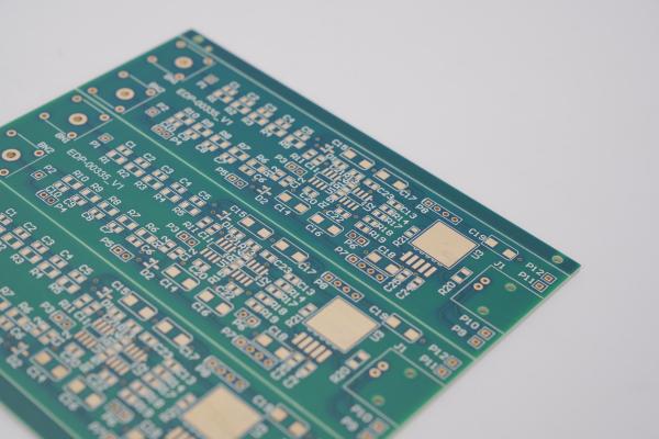
High Frequency Signal PCB Manufacturing Challenges
High Frequency Signal PCB manufacturing requires strict control of process capability and tolerances. Key challenges include:
-
Tight etching tolerance for trace width and spacing
-
Stable dielectric thickness control for impedance accuracy
-
Copper roughness control to reduce conductor loss
-
Multilayer lamination stability and registration accuracy
-
Reliable via plating and hole wall quality
-
Controlled impedance testing and verification
High frequency PCB manufacturing quality directly impacts insertion loss, return loss, and overall RF performance.
KKPCB High Frequency Signal PCB Capabilities
KKPCB provides professional High Frequency Signal PCB manufacturing with engineering support from design review to mass production. Our capabilities include:
-
Controlled impedance High Frequency Signal PCB fabrication
-
Low-loss material support (Rogers, PTFE, Megtron, hybrid stack-ups)
-
Multilayer high frequency PCB manufacturing
-
Fine line routing for compact RF modules
-
High reliability inspection, AOI, and electrical testing
-
Engineering support for stack-up planning and DFM optimization
KKPCB helps customers build High Frequency Signal PCBs with consistent performance, stable impedance, and reliable production quality.
Conclusion
A High Frequency Signal PCB is essential for modern electronics requiring low loss transmission, controlled impedance, and stable signal integrity at high frequency. By selecting the right materials, optimizing stack-up design, controlling impedance, and improving grounding and via transitions, High Frequency Signal PCBs deliver reliable performance for RF, microwave, 5G, and high-speed applications.
KKPCB supports high-quality High Frequency Signal PCB manufacturing with advanced engineering capability and strict process control, helping customers achieve stable high frequency signal performance from prototype to mass production.
