What Is a High Speed Logic PCB?
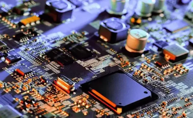
A High Speed Logic PCB is a printed circuit board engineered to handle high-frequency digital signals with minimal distortion, noise, or timing errors. These PCBs are critical in applications where fast signal transitions, high data rates, and precise timing are required, such as computer motherboards, networking equipment, 5G digital modules, and high-performance microcontrollers.
High Speed Logic PCBs focus on signal integrity (SI), controlled impedance, differential pair routing, and proper power delivery to ensure reliable operation of complex digital systems.
Why High Speed Logic PCBs Are Important
Without proper high-speed PCB design, systems may suffer from:
-
Signal reflections and ringing
-
Crosstalk between adjacent traces
-
Timing skew and data errors
-
EMI and reduced signal quality
A well-designed High Speed Logic PCB ensures clean signal transmission, predictable timing, and high reliability in demanding digital environments.
Key Design Considerations for High Speed Logic PCBs
1. Controlled Impedance Routing
Maintaining consistent trace impedance is essential to prevent reflections and signal loss in high-speed digital circuits. Controlled impedance ensures signal fidelity and timing accuracy.
2. Differential Pair Design
Interfaces like USB, PCIe, SATA, and Ethernet rely on differential pairs. Proper spacing, length matching, and symmetry reduce noise and crosstalk, improving signal integrity.
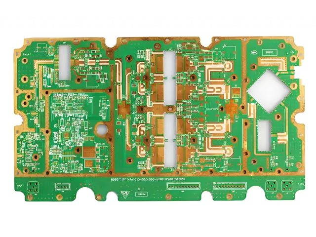
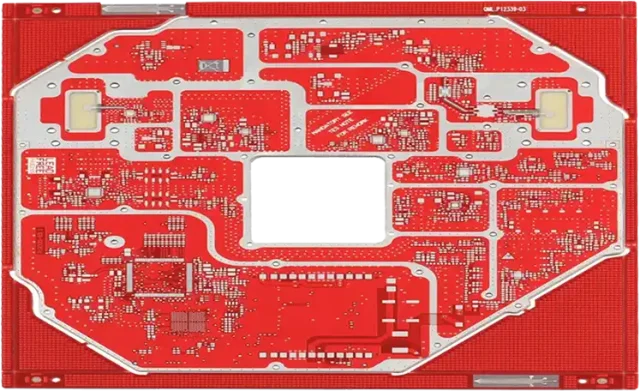
3. Multilayer Stack-Up Optimization
High-speed PCBs benefit from dedicated signal, ground, and power planes, which provide stable return paths, reduce EMI, and improve power delivery.
4. Crosstalk and Noise Mitigation
Routing high-speed signals carefully, maintaining trace separation, and using proper layer assignments minimize crosstalk and noise.
5. Low-Loss Materials
Using low-loss laminates preserves signal strength at high frequencies, critical for data centers, 5G modules, and RF/digital hybrid systems.
6. Thermal and Power Management
High-speed logic circuits often generate heat. Proper thermal vias, plane allocation, and power delivery optimization maintain signal stability and PCB reliability.
Applications of High Speed Logic PCBs
-
High-speed computing and server motherboards
-
Networking equipment and data transmission systems
-
5G digital front-end modules
-
IoT devices and edge computing electronics
-
Automotive ECUs and advanced driver-assistance systems (ADAS)
-
Semiconductor testing and digital measurement systems
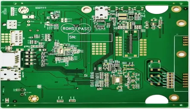
KKPCB High Speed Logic PCB Capabilities
KKPCB offers professional design and manufacturing services for High Speed Logic PCBs, including:
-
Controlled impedance and differential pair routing
-
Multilayer PCB fabrication with optimized stack-ups
-
Low-loss material selection and high-density routing
-
Signal integrity testing and high-speed validation
-
Small batch prototyping to full-scale production
Our team ensures that High Speed Logic PCBs meet stringent electrical, thermal, and mechanical requirements, delivering reliable, high-performance digital solutions.
Conclusion
A High Speed Logic PCB is essential for modern digital electronics requiring high data rates, precise timing, and reliable signal transmission. Through controlled impedance, optimized stack-ups, low-loss materials, and careful signal routing, KKPCB delivers professional High Speed Logic PCB solutions for computing, networking, 5G, automotive, and semiconductor applications.
