Introduction to Microvia PCB
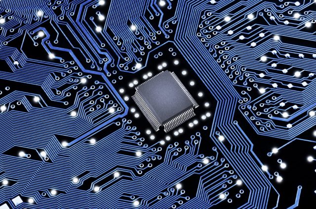
A Microvia PCB is a key enabling technology in HDI (High Density Interconnect) PCB manufacturing, designed to meet the increasing demands for miniaturization, high-speed signal transmission, and high component density. By using laser-drilled microvias, Microvia PCBs significantly reduce interconnect length, improve routing flexibility, and enhance overall electrical performance.
Microvia PCB technology is widely adopted in smartphones, wearable devices, high-speed computing, automotive electronics, medical equipment, and semiconductor test systems, where compact size and high reliability are essential.
What Is a Microvia?
A microvia is a small-diameter via, typically ≤150 μm, created using laser drilling instead of mechanical drilling. Microvias are commonly used to connect:
-
Adjacent layers (L1–L2, L2–L3)
-
Sequential buildup layers in HDI PCB structures
Unlike traditional through-hole vias, microvias reduce parasitic inductance and capacitance, resulting in better signal integrity and power integrity.
Key Advantages of Microvia PCB
Microvia PCBs offer several critical benefits for advanced electronic designs:
-
Higher wiring density for complex layouts
-
Shorter signal paths, improving high-speed performance
-
Lower parasitic effects, ideal for RF and high-frequency applications
-
Improved thermal performance due to reduced via size
-
Smaller board size, supporting compact and lightweight devices
These advantages make Microvia PCB technology essential for fine-pitch BGA, CSP, and flip-chip packages.
Types of Microvia Structures
Depending on design requirements, Microvia PCBs can be fabricated using different structures:
-
Stacked Microvias – Vertical alignment for high-density vertical interconnection
-
Staggered Microvias – Offset structure for improved mechanical reliability
-
Via-in-Pad Microvia – Microvias placed directly in component pads, often filled and plated
Each structure is selected based on signal speed, layer count, reliability, and cost considerations.
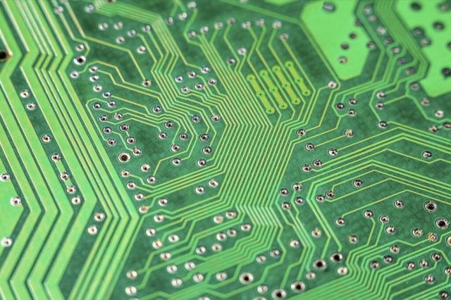
Microvia PCB Manufacturing Process
The manufacturing of Microvia PCBs requires advanced equipment and strict process control, including:
-
Laser drilling for precise microvia formation
-
Desmear and surface treatment to ensure clean via walls
-
Copper plating for reliable electrical connection
-
Via filling (conductive or non-conductive) for via-in-pad designs
-
Sequential lamination for multilayer HDI buildup
Strict inspection methods such as AOI, X-ray inspection, and electrical testing are applied to guarantee quality and reliability.
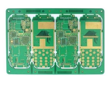
Applications of Microvia PCB
Microvia PCBs are widely used in industries that demand high performance and compact design, including:
-
Consumer electronics (smartphones, tablets, wearables)
-
High-speed servers and networking equipment
-
Automotive electronics and ADAS systems
-
Medical and industrial electronics
-
Semiconductor test boards and IC testing PCBs
Microvia PCB technology is especially critical for high-speed digital, RF, and mixed-signal applications.
Why Choose KKPCB for Microvia PCB Manufacturing
KKPCB provides advanced Microvia PCB fabrication services, supporting:
-
HDI PCB up to high layer counts
-
Stacked and staggered microvia designs
-
Via-in-pad filling and planarization
-
Tight impedance control and fine line spacing
-
Reliable small-batch prototyping and volume production
With experienced engineering support and strict quality control, KKPCB ensures high-reliability Microvia PCBs for demanding applications.
Conclusion
As electronic devices continue to shrink while performance requirements increase, Microvia PCB technology has become indispensable. By enabling high-density interconnection, superior signal integrity, and compact layouts, Microvia PCBs play a vital role in modern electronics and semiconductor testing solutions.
