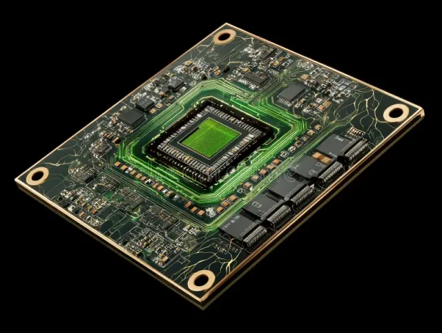
What Is a High Speed Logic PCB?

A High Speed Logic PCB is a printed circuit board engineered to support high-frequency digital signals in modern electronic systems. It ensures signal integrity, controlled impedance, and minimal noise, enabling reliable operation in FPGA, CPU, memory modules, and high-performance digital logic circuits.
High speed logic PCBs are essential in applications where data rates exceed hundreds of megahertz to several gigahertz, such as 5G infrastructure, high-speed computing, networking devices, and advanced IoT systems.
Key Challenges in High Speed Logic PCB Design
Designing a High Speed Logic PCB involves addressing several critical challenges:
-
Signal integrity: Maintaining clean signals at high frequency to avoid reflection, crosstalk, and jitter
-
Controlled impedance: Ensuring trace width, spacing, and stackup deliver precise impedance
-
Low noise and EMI: Minimizing electromagnetic interference in densely packed digital circuits
-
High-density routing: Managing fine-pitch components, BGA, QFN, and high pin-count ICs
-
Thermal management: Handling heat from high-speed chips without degrading performance
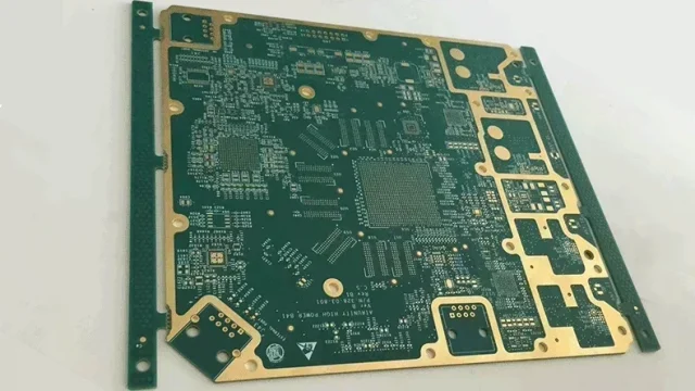
Design Principles for High Speed Logic PCB
1. Controlled Impedance and Signal Routing
Trace width, spacing, and layer stacking are carefully calculated to maintain 50Ω or differential impedance, ensuring high-speed signals propagate cleanly without distortion.
2. Optimized Layer Stack-Up
High speed logic PCBs often use multilayer stack-ups with dedicated power and ground planes, providing clean return paths and minimizing crosstalk and noise.
3. Differential Pair and Length Matching
Differential pairs are routed with precise length matching, and critical signals are isolated to prevent skew, jitter, and timing errors in high-speed circuits.
4. Low Loss PCB Materials
High frequency laminates and low dielectric loss materials are used to reduce signal attenuation and phase distortion in high-speed logic traces.
5. Decoupling and Power Integrity
Proper placement of decoupling capacitors and robust power plane design ensures stable voltage delivery to high-speed logic devices.
Applications of High Speed Logic PCBs
High Speed Logic PCBs are widely applied in:
-
FPGA and CPU boards
-
High-speed memory modules (DDR4/DDR5, LPDDR)
-
High-speed data acquisition and networking systems
-
5G infrastructure and baseband modules
-
Automotive electronic control units (ECU) and ADAS
-
Industrial automation and robotics
KKPCB High Speed Logic PCB Capabilities
KKPCB provides full-service High Speed Logic PCB solutions, including:
-
Precision controlled impedance PCB fabrication
-
Multilayer PCB stack-up design for high-speed logic circuits
-
Use of low loss and high Tg materials for signal integrity
-
Professional layout support for high pin-count and fine-pitch components
-
Rigorous electrical testing, signal integrity verification, and quality inspection
KKPCB ensures every High Speed Logic PCB meets the strictest electrical performance and reliability standards, from prototype to mass production.
Conclusion

A well-designed High Speed Logic PCB is critical for modern high-performance digital systems. Through controlled impedance, optimized layer stack-ups, low loss materials, and careful signal routing, these PCBs enable reliable operation of FPGA, CPU, memory, and high-speed digital circuits.
For your next high-speed digital project, KKPCB offers expert design support and high-quality High Speed Logic PCB manufacturing to meet demanding performance requirements.
