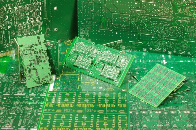
A Multilayer PCB is a printed circuit board composed of three or more layers of conductive traces separated by insulating substrates, allowing more complex circuitry, higher routing density, and superior signal integrity. Multilayer PCBs are widely used in high-speed computing, RF communication, IoT, semiconductor testing, and automotive systems, where compact size and high performance are critical.
Key Features of Multilayer PCBs
1. Multiple Signal, Power, and Ground Layers
Multilayer PCBs provide separate layers for signal routing, power distribution, and grounding, reducing crosstalk, EMI, and noise, and improving overall electrical performance.
2. High-Density Interconnect (HDI) and Microvia Technology
HDI and microvia structures allow for shorter signal paths, high routing density, and support for fine-pitch ICs, essential for high-speed and high-frequency circuits.
3. Controlled Impedance and Signal Integrity
By precisely controlling trace width, spacing, and dielectric thickness, multilayer PCBs maintain consistent impedance, ensuring reliable signal transmission for RF, high-speed digital, and 5G applications.
4. Compact Form Factor
Multilayer designs enable smaller PCB footprints without sacrificing functionality, making them ideal for IoT devices, wearable electronics, and automotive modules.
5. Thermal and Mechanical Reliability
Advanced materials and lamination processes ensure mechanical strength, thermal stability, and long-term reliability under harsh operating conditions.
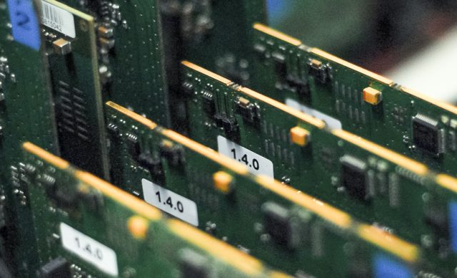
Applications of Multilayer PCBs
Multilayer PCBs are essential for modern electronic systems requiring high performance, miniaturization, and reliability:
-
High-speed computing and networking equipment
-
5G and RF communication modules
-
IoT and wearable electronics
-
Automotive ECUs, ADAS, and radar modules
-
Semiconductor IC test boards and ATE systems
-
Medical and industrial compact electronics
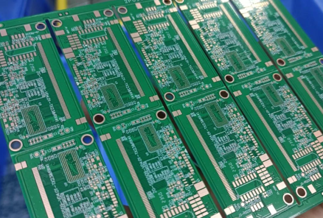
Manufacturing Considerations
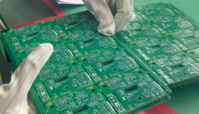
Manufacturing multilayer PCBs involves precision processes to ensure performance and reliability:
-
Accurate layer alignment and lamination
-
Controlled copper plating and via formation
-
High-quality surface finishes and soldermask application
-
Microvias, blind, and buried vias for HDI multilayer boards
-
AOI, X-ray, and electrical testing to guarantee performance
These steps ensure stable electrical performance, high yield, and long-term reliability.
Conclusion
Multilayer PCBs are the backbone of modern high-performance electronics, providing high-density routing, superior signal integrity, and reliable power distribution. From RF and 5G applications to IoT, automotive, and semiconductor testing, multilayer PCB technology supports compact, efficient, and robust electronic designs.
