What Is a Microvia PCB?
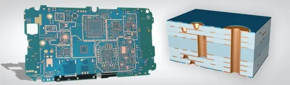
A Microvia PCB is an advanced type of HDI (High Density Interconnect) printed circuit board that uses laser-drilled microvias, typically with a diameter of ≤150 μm, to interconnect PCB layers. Unlike traditional mechanical vias, microvias are designed for shorter signal paths, higher routing density, and compact layouts, making them essential for modern electronics.
Microvia PCBs are widely used in applications requiring miniaturization, high-speed signal transmission, and high pin count IC integration.
Types of Microvias in PCB Manufacturing
Microvia PCB technology includes several via structures depending on design requirements:
-
Blind Microvias – Connect outer layers to inner layers
-
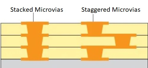
Stacked Microvias – Vertically aligned microvias for ultra-high density
-
Staggered Microvias – Offset microvias to improve reliability
-
Via-in-Pad Microvias – Placed directly in component pads for fine-pitch BGAs
These microvia structures enable HDI PCB designs with exceptional routing flexibility.
Advantages of Microvia PCB Technology
Using a Microvia PCB provides multiple performance and design benefits:
-
Extremely high wiring density for compact layouts
-
Improved signal integrity with reduced parasitic effects
-
Shorter interconnection paths for high-speed and RF signals
-
Support for fine-pitch, high pin count components
-
Reduced PCB size and layer count optimization
-
Enhanced electrical performance for GHz-level applications
These advantages make microvia PCBs a core technology for advanced electronics.
Applications of Microvia PCBs
Microvia PCBs are widely applied across high-end electronic industries:
-
HDI PCBs for smartphones and wearable devices
-
Semiconductor test PCBs and ATE test boards
-
High-speed digital and controlled impedance PCBs
-
RF, microwave, and 5G communication modules
-
Automotive electronics and ADAS systems
-
Medical devices and compact industrial equipment
As device density increases, Microvia PCB designs become indispensable.
Microvia PCB Manufacturing Process
Producing a high-reliability Microvia PCB requires advanced manufacturing capabilities:
-
Laser drilling for precise microvia formation
-
Sequential lamination for HDI stack-ups
-
High-quality copper filling and plating
-
Tight layer-to-layer registration control
-
AOI, X-ray inspection, and electrical testing
Process control is critical to ensure microvia reliability, especially for stacked microvia structures.
Design Considerations for Microvia PCBs
Successful Microvia PCB design involves careful engineering planning:
-
Proper microvia aspect ratio control
-
Optimized HDI stack-up planning
-
Controlled impedance routing for high-speed signals
-
Thermal stress and reliability evaluation
-
Compatibility with fine-pitch BGA and CSP packages
Early DFM and DFT involvement helps reduce cost and improve yield.
Microvia PCB vs Traditional Via PCB
Compared with conventional through-hole vias, Microvia PCBs offer:
-
Smaller via size and higher density
-
Better electrical performance
-
Greater design freedom for compact products
-
Improved support for advanced IC packaging
For high-speed and high-density electronics, microvia technology is often the preferred choice.
Why Choose Microvia PCBs for Advanced Electronics?
Microvia PCBs enable:
-
Next-generation HDI designs
-
Reliable performance in high-speed and RF circuits
-
Compact and lightweight electronic products
-
Scalability from prototype to mass production
They are a key foundation for today’s and tomorrow’s electronic systems.
