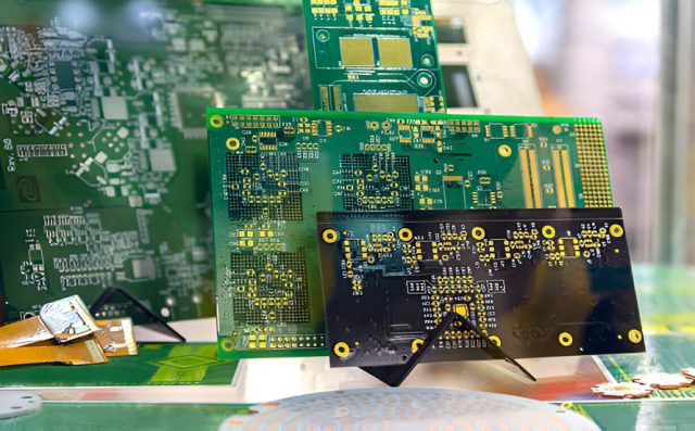
A Multilayer PCB is a printed circuit board composed of three or more conductive copper layers laminated together with insulating materials. As electronic products continue to demand higher functionality, faster signal speeds, and smaller form factors, multilayer PCBs have become the backbone of advanced electronics, semiconductor testing, communication systems, and industrial control equipment.
Compared with single-layer or double-layer boards, multilayer PCBs provide greater routing density, improved signal integrity, and enhanced electrical performance.
Why Multilayer PCBs Are Essential
Modern electronic systems integrate high-speed digital signals, RF circuits, power management, and sensitive analog components on a single board. A multilayer PCB enables:
-
Higher circuit density in limited space
-
Shorter signal paths and reduced parasitics
-
Better power and ground distribution
-
Lower EMI and crosstalk
-
Improved reliability and mechanical stability
These advantages make multilayer PCBs indispensable for high-performance and mission-critical applications.
Key Structural Features of Multilayer PCBs
1. Optimized Layer Stackup
A well-designed multilayer PCB stackup separates signal layers, power planes, and ground planes, ensuring controlled impedance and stable return paths.
2. Dedicated Power and Ground Planes
Internal planes reduce voltage drop and noise, providing clean power delivery and improved signal integrity for high-speed and mixed-signal designs.
3. Advanced Via Technology
Multilayer PCBs often incorporate blind vias, buried vias, and microvias to maximize routing efficiency and support HDI designs.
4. Controlled Impedance Routing
Precise trace geometry and dielectric thickness allow accurate impedance control, essential for high-speed digital and RF circuits.
5. High-Precision Lamination Process
Multiple lamination cycles ensure layer alignment, structural stability, and consistent electrical performance.
Advantages of Multilayer PCBs
-
High wiring density and compact design
-
Improved signal integrity for high-speed applications
-
Reduced electromagnetic interference (EMI)
-
Enhanced thermal distribution
-
Better mechanical strength and durability
-
Support for complex and multifunctional systems
These benefits make multilayer PCBs ideal for both prototype development and volume production.
Applications of Multilayer PCBs
Multilayer PCBs are widely used across industries, including:
-
Semiconductor testing PCBs and ATE load boards
-
High-speed IC test and probe card systems
-
5G communication and networking equipment
-
RF and microwave modules
-
Industrial automation and control systems
-
Medical electronics and diagnostic devices
-
Automotive electronics and ADAS systems
-
High-performance computing and data centers
In these applications, PCB layer count directly impacts performance, stability, and scalability.
Manufacturing Challenges and Requirements
Producing reliable multilayer PCBs requires advanced capabilities, including:
-
Precise layer registration and alignment
-
Tight thickness and impedance control
-
High-quality lamination materials
-
Strict process control for multilayer drilling and plating
-
Comprehensive electrical and reliability testing
An experienced multilayer PCB manufacturer ensures consistent quality, high yield, and dependable long-term performance.
Conclusion
A Multilayer PCB is the foundation of modern high-density, high-speed, and multifunctional electronic systems. By enabling complex routing, controlled impedance, stable power distribution, and superior signal integrity, multilayer PCBs support the growing demands of semiconductor testing, communication technology, and advanced electronics.
Choosing the right multilayer PCB partner ensures design flexibility, manufacturing reliability, and scalable production, from early prototypes to mass manufacturing.
