High Layer Count PCB: The Backbone of Complex Electronic Systems
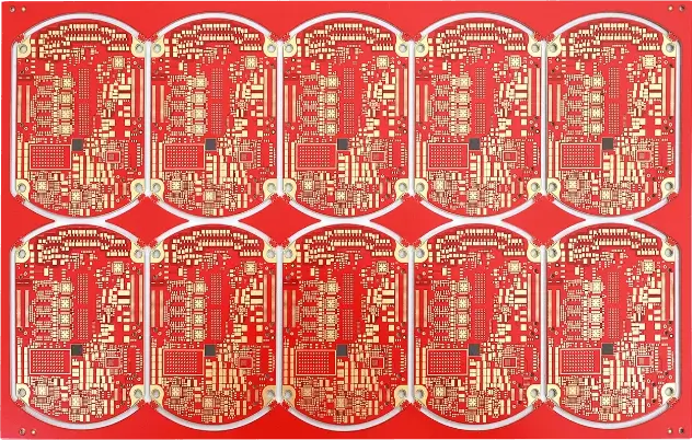
A High Layer Count PCB refers to a multilayer printed circuit board typically featuring 16 layers, 24 layers, 32 layers, or more, designed to support complex signal routing, dense interconnections, and advanced power distribution. As electronic systems continue to integrate higher data rates, tighter form factors, and mixed-signal architectures, High Layer Count PCB designs have become essential for maintaining electrical performance and mechanical stability.
High layer count PCBs are widely used in servers, networking equipment, telecom infrastructure, aerospace systems, industrial control, and high-performance computing platforms, where routing density and signal integrity requirements exceed the limits of conventional multilayer boards.
Why High Layer Count PCB Is Essential for Modern Electronics
As IC pin counts increase and interface speeds move into multi-gigabit and RF domains, traditional low-layer PCBs struggle to meet routing and performance demands. High Layer Count PCB architectures provide the vertical routing capacity required to separate signal, power, and ground planes effectively.
Key benefits of High Layer Count PCB designs include:
-
Increased routing density without trace congestion
-
Dedicated signal, power, and ground layers for improved isolation
-
Enhanced power integrity through distributed reference planes
-
Reduced electromagnetic interference (EMI)
-
Improved signal integrity for high-speed and high-frequency interfaces
By expanding the layer stack vertically, High Layer Count PCBs enable cleaner layouts and more predictable electrical behavior.
Signal Integrity Advantages of High Layer Count PCB Stackups
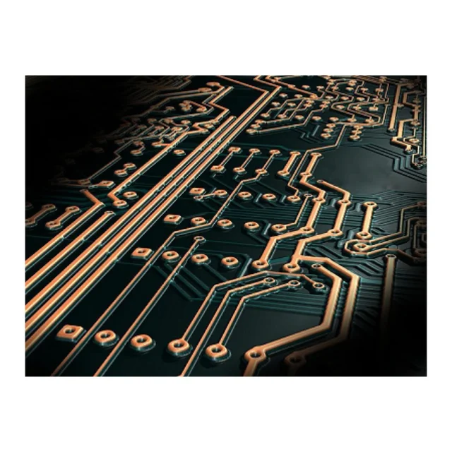
Signal integrity is one of the primary drivers behind High Layer Count PCB adoption. With additional layers, designers can allocate continuous reference planes close to high-speed signal layers.
From an SI perspective, High Layer Count PCBs offer:
-
Tighter controlled impedance routing
-
Reduced crosstalk through layer-to-layer isolation
-
Shorter return current paths
-
Lower insertion loss and reflection
-
Improved timing margin for multi-gigabit signals
These advantages are critical for PCIe, Ethernet, SerDes, DDR, and high-speed backplane applications, where signal degradation directly impacts system reliability.
Power Integrity and Grounding in High Layer Count PCBs
High current consumption and fast switching devices demand robust power delivery networks. High Layer Count PCB designs allow multiple power and ground planes to be strategically placed throughout the stackup.
Key power integrity benefits include:
-
Lower PDN impedance across wide frequency ranges
-
Reduced voltage ripple and ground bounce
-
Improved decoupling capacitor effectiveness
-
Stable reference planes for sensitive analog and RF circuits
By distributing power planes across the stack, High Layer Count PCBs maintain voltage stability even under dynamic load conditions.
High Layer Count PCB Stackup Engineering
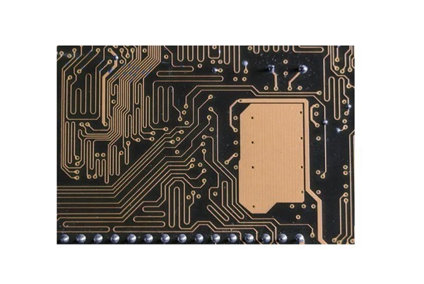
Designing a reliable High Layer Count PCB stackup requires careful planning of layer sequence, symmetry, and material selection.
Typical stackup considerations include:
-
Balanced layer construction to minimize warpage
-
Alternating signal and reference plane layers
-
Low-loss dielectric materials for high-speed layers
-
Controlled dielectric thickness for impedance accuracy
-
Segregation of digital, analog, and RF domains
Poor stackup design can result in signal integrity issues, delamination, or manufacturing yield loss. Proper High Layer Count PCB engineering ensures electrical performance and mechanical stability coexist.
Manufacturing Challenges of High Layer Count PCBs
As layer count increases, fabrication complexity rises exponentially. High Layer Count PCB manufacturing demands tight control over every process step.
Major challenges include:
-
Precise layer-to-layer registration
-
Uniform lamination pressure across thick stacks
-
Drilling accuracy for deep via structures
-
Reliable plated through-hole integrity
-
Prevention of resin starvation and delamination
Because rework is nearly impossible, High Layer Count PCB fabrication requires advanced equipment, experienced process control, and rigorous inspection.
Thermal and Mechanical Reliability of High Layer Count PCBs
High Layer Count PCBs often operate in thermally demanding environments. Thick stacks with dense copper structures must manage thermal expansion and heat dissipation effectively.
Reliability advantages include:
-
Improved heat spreading through internal copper planes
-
Enhanced resistance to thermal cycling fatigue
-
Reduced mechanical stress on solder joints
-
Long-term dimensional stability
When properly engineered, High Layer Count PCBs deliver consistent performance across wide temperature ranges.
Applications of High Layer Count PCB Technology
High Layer Count PCBs are commonly deployed in:
-
Data center servers and switches
-
5G base stations and telecom backplanes
-
Aerospace and defense electronics
-
Industrial automation controllers
-
High-performance computing systems
In these systems, High Layer Count PCB solutions enable scalability, reliability, and electrical performance at the system level.
KKPCB High Layer Count PCB Capabilities
KKPCB specializes in High Layer Count PCB engineering and manufacturing, offering:
-
Custom multilayer stackup design and DFM support
-
High-precision layer alignment and lamination
-
Controlled impedance routing for high-speed signals
-
Low-loss material options for critical layers
-
Prototype to mass production scalability
Each High Layer Count PCB is built to meet stringent electrical, mechanical, and reliability requirements.
Conclusion
A High Layer Count PCB is a critical enabler for modern electronic systems requiring high routing density, robust power integrity, and superior signal integrity. By leveraging advanced stackup design and precision manufacturing, High Layer Count PCBs unlock performance levels unattainable with lower-layer boards.
KKPCB delivers reliable High Layer Count PCB solutions through deep engineering expertise, advanced fabrication capabilities, and strict quality control—supporting complex electronic designs from concept to volume production.
