High Layer Count PCB: The Backbone of Ultra-Complex Electronic Integration
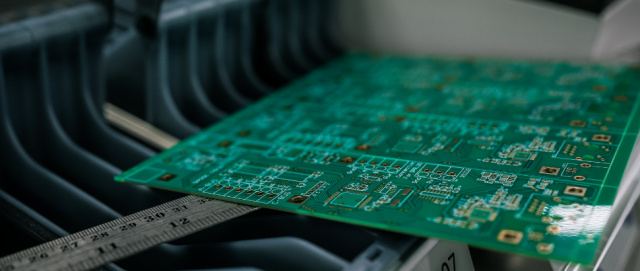
A High Layer Count PCB refers to a multilayer printed circuit board typically exceeding 12 layers and extending to 20, 30, or even 60+ layers for advanced electronic systems. High layer count PCB designs are essential for applications requiring dense routing, high-speed signal transmission, controlled impedance, and robust power distribution within limited board real estate.
As system integration levels continue to rise, High Layer Count PCB architectures have become a foundational technology for data centers, telecommunications infrastructure, aerospace electronics, medical imaging systems, and high-performance computing platforms.
Why High Layer Count PCB Designs Are Critical
Modern electronic systems integrate high-speed digital interfaces, RF circuits, power management networks, and sensitive analog signals on a single board. A High Layer Count PCB enables functional partitioning by dedicating individual layers to signals, power planes, and ground references.
Key advantages of High Layer Count PCB designs include:
-
Increased routing density for complex IC fan-out
-
Dedicated power and ground planes for low-impedance PDN
-
Superior signal integrity for high-speed and high-frequency traces
-
Reduced EMI through optimized reference planes
-
Compact system layout without performance compromise
Without High Layer Count PCB technology, many advanced electronic systems would be physically impossible to implement.
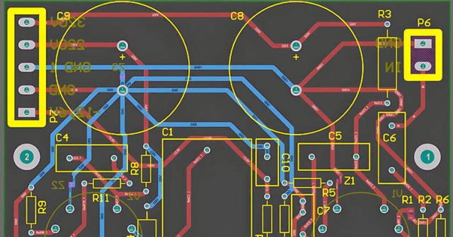
Signal Integrity Challenges in High Layer Count PCB Systems
As layer count increases, maintaining signal integrity becomes more complex. High Layer Count PCB engineering must address challenges such as impedance discontinuities, via stubs, crosstalk, and skew control.
Critical signal integrity considerations include:
-
Tight dielectric thickness control for impedance consistency
-
Back-drilling or blind/buried vias to reduce via stubs
-
Differential pair phase matching across multiple layers
-
Low-loss dielectric materials for high-speed and RF layers
-
Controlled return paths using continuous reference planes
A well-designed High Layer Count PCB ensures stable eye diagrams, low jitter, and predictable high-speed performance.
Power Integrity and Thermal Management in High Layer Count PCB Designs
High-performance systems demand stable power delivery. High Layer Count PCB stackups allow designers to integrate multiple power planes close to signal layers, minimizing loop inductance and voltage ripple.
Thermal performance is equally critical. A High Layer Count PCB supports:
-
Embedded copper planes for heat spreading
-
Via-in-pad and thermal via arrays
-
Balanced copper distribution to reduce warpage
-
High-Tg and low-CTE materials for thermal reliability
Effective power and thermal engineering ensure long-term reliability in high-power, high-density environments.
Material Selection for High Layer Count PCB Fabrication
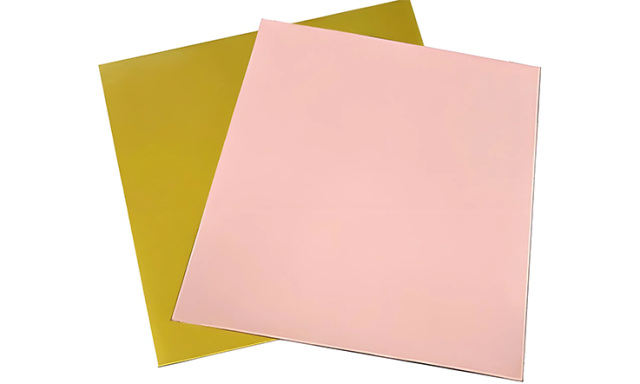
Material selection directly impacts electrical stability and manufacturability. High Layer Count PCB materials are chosen based on signal speed, operating frequency, and thermal stress.
Common material systems include:
-
High-Tg FR-4 for digital and mixed-signal layers
-
Low-loss laminates for high-speed and RF layers
-
Hybrid stackups combining RF and standard materials
-
Low-CTE prepregs for dimensional stability
Precise lamination control is essential to prevent resin starvation, delamination, and layer misregistration in High Layer Count PCB manufacturing.
Manufacturing Complexity of High Layer Count PCBs
Fabricating a High Layer Count PCB requires advanced process control and engineering expertise. As layer count increases, tolerances become tighter and yield risks rise.
Key manufacturing challenges include:
-
Multi-stage sequential lamination
-
Registration accuracy across dozens of layers
-
Drill accuracy for deep aspect-ratio vias
-
Uniform copper plating across thick stacks
-
AOI and electrical testing at each lamination stage
Only manufacturers with proven High Layer Count PCB fabrication capabilities can consistently deliver reliable results.
High Layer Count PCB Applications
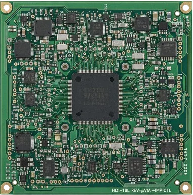
High Layer Count PCB technology is widely used in:
-
Data center switches and servers
-
5G base stations and core network equipment
-
Aerospace avionics and satellite payloads
-
Medical imaging and diagnostic platforms
-
High-performance computing and AI accelerators
In these systems, High Layer Count PCBs enable performance scaling without increasing board size.
KKPCB High Layer Count PCB Capabilities
KKPCB provides end-to-end High Layer Count PCB manufacturing and engineering support, including:
-
Multilayer PCB fabrication up to ultra-high layer counts
-
Blind, buried, and back-drilled via technologies
-
Controlled impedance and low-loss stackup design
-
Hybrid material lamination
-
DFM, DFI, and signal integrity review
From prototype to mass production, KKPCB ensures High Layer Count PCB reliability, electrical consistency, and manufacturability.
Conclusion
A High Layer Count PCB is not simply a thicker circuit board—it is a carefully engineered system platform. Through advanced stackup design, material optimization, and precision manufacturing, High Layer Count PCB architectures enable ultra-complex routing, stable signal integrity, and robust power delivery in next-generation electronics.
For applications demanding density, performance, and reliability, High Layer Count PCB solutions are indispensable. KKPCB delivers the engineering depth and production control required to support these demanding designs.
