Introduction: Why PCB Prototype Engineering Defines Modern Electronics
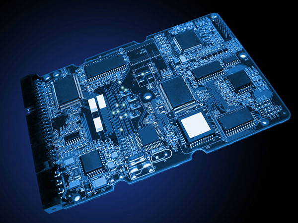
A PCB Prototype is no longer just a pre-production sample—it is the central engineering stage that determines product performance, manufacturability, reliability, and cost.
In advanced electronics such as 5G, IoT, robotics, automotive, aerospace, AI edge computing, and industrial automation, a well-engineered PCB Prototype ensures signal integrity, thermal stability, and system longevity before scaling into mass production.
Today, the PCB Prototype is the foundation of high-speed digital design, RF/mmWave communication, HDI integration, and power-dense applications.
1. Engineering Requirements of a High-Performance PCB Prototype
Developing a professional PCB Prototype involves precise engineering control across multiple domains:
1.1 High-Speed Signal Integrity
A modern PCB Prototype must support high-speed interfaces such as:
-
PCIe Gen4/5/6
-
USB 3.2 / USB4
-
SerDes 25–112 Gbps
-
MIPI D-PHY / C-PHY
To achieve stability, the PCB Prototype must implement: -
Controlled impedance (±5% or better)
-
Trace length matching
-
Low-loss dielectric materials
-
Optimized reference plane structure
1.2 HDI and Miniaturization
As devices shrink, the PCB Prototype requires:
-
Laser microvias
-
Stack-up optimization
-
25–50 μm dielectrics
-
Fine line/space (50–75 μm)
HDI-focused PCB Prototype engineering allows higher IO density and compact system integration.
1.3 Thermal and Power Management
Power-dense designs require PCB Prototype solutions with:
-
High-thermal laminates
-
Copper balancing
-
Thermal vias
-
MCPCB or ceramic substrates
This ensures that the PCB Prototype performs reliably under continuous high-load conditions.
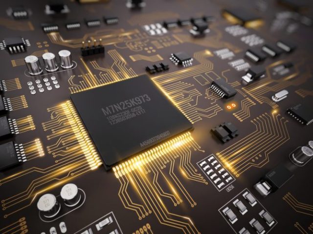
2. Advanced Materials in PCB Prototype Development
Material selection determines the electrical and thermal performance of a PCB Prototype:
Low-Loss RF Materials
Used for 5G, radar, satellite:
-
Rogers 4350B/4003C
-
Megtron 6/7
-
Taconic
These ensure low signal attenuation across GHz/mmWave frequencies.
High-Thermal Substrates
Ideal for power modules and robotics:
-
Aluminum Nitride (AlN)
-
Aluminum Oxide (Al₂O₃)
-
Metal-Core PCBs
Pairing these materials with the PCB Prototype stage ensures early thermal validation before mass production.
Ultra-Thin HDI Laminates
Enable fine-pitch BGA, camera modules, AI processors, etc.
A well-designed PCB Prototype validates manufacturability and interconnect reliability before costly tooling.
3. Stack-Up Engineering: The Heart of the PCB Prototype
The stack-up defines how a PCB Prototype handles:
-
Differential impedance
-
Layer registration
-
Signal return paths
-
Crosstalk
-
EMI/EMC behavior
Engineering teams must validate each PCB Prototype with:
-
Dielectric height accuracy
-
Copper weight uniformity
-
Controlled plane distribution
-
High-frequency simulation
A well-constructed stack-up enables consistent performance when the PCB Prototype transitions to production.
4. Manufacturing Tolerances in PCB Prototype Fabrication
Precision tolerances are essential to ensure the PCB Prototype represents true production behavior.
Key Tolerances
-
Layer-to-layer registration ±75 μm
-
Copper thickness uniformity 1 oz ±10%
-
Microvia diameter ≤ 75 μm
-
Trace width/space consistency
A precision-built PCB Prototype allows early detection of fabrication limitations and avoids costly redesign cycles.
5. Testing and Validation of the PCB Prototype
No PCB Prototype is complete without full engineering validation.
Electrical Tests
-
Impedance verification
-
S-parameter measurement (for RF)
-
Time-domain reflectometry (TDR)
Reliability Tests
-
Thermal cycling
-
Solder joint reliability
-
Microvia inspection
-
Warpage control
These tests ensure that the PCB Prototype can transition directly into mass production with confidence.
6. Why High-Quality PCB Prototypes Reduce Cost and Time-to-Market
A professional PCB Prototype prevents:
-
Redesign iterations
-
Unexpected EMI failures
-
Signal integrity degradation
-
Over-heating issues
-
Component incompatibility
A well-engineered PCB Prototype leads to:
-
Faster product development
-
Higher production yield
-
More stable long-term operation
-
Lower lifetime manufacturing cost
Thus, the PCB Prototype stage is not optional—it is the core of successful product engineering.
Conclusion
The PCB Prototype is the engineering backbone of every modern electronic product.
By integrating advanced materials, HDI structures, controlled impedance routing, tight-tolerance manufacturing, and comprehensive validation, a PCB Prototype becomes a reliable platform for innovation.
Whether for high-speed digital, RF/mmWave, embedded computing, robotics, satellite technology, EV systems, or medical electronics, mastering PCB Prototype engineering is essential for unlocking next-generation performance.
