5G millimeter-wave (mmWave) technology operates at extremely high frequencies, typically above 24 GHz, where traditional PCB materials and design rules are no longer sufficient. The 5G mmWave PCB is a specialized high-frequency printed circuit board engineered to minimize signal loss, maintain phase stability, and support compact antenna integration required for next-generation wireless communication systems.
A well-designed 5G mmWave PCB is essential for achieving the performance targets of 5G base stations, small cells, and user equipment.
What Is a 5G mmWave PCB?
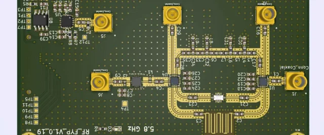
A 5G mmWave PCB is a high-frequency PCB designed specifically for millimeter-wave communication bands used in 5G systems. It supports:
-
RF front-end modules
-
Phased-array antennas
-
High-speed transceivers and beamforming circuits
These PCBs must maintain stable performance at extremely short wavelengths.
Why mmWave Frequencies Demand Specialized PCB Design
At mmWave frequencies, even small PCB variations can cause:
-
Significant insertion loss
-
Phase shift and timing error
-
Impedance mismatch and reflection
The 5G mmWave PCB is designed to control these effects through material selection and precision manufacturing.
Low-Loss Material Selection for 5G mmWave PCBs
Material choice is critical at mmWave frequencies. Common materials include:
-
Rogers RT/duroid® laminates
-
RO4003 and RO3003 series
-
Hybrid stackups combining PTFE and FR-4
Low dielectric loss and stable Dk are essential for mmWave signal integrity.
Controlled Impedance and Phase Stability
Precise impedance control is mandatory for mmWave designs. A 5G mmWave PCB ensures:
-
Accurate transmission line geometry
-
Tight dielectric thickness tolerance
-
Stable phase response across temperature and frequency
Phase consistency is especially important for beamforming systems.
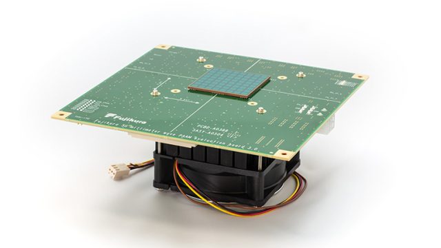
Antenna Integration and Array Design
Many 5G mmWave PCBs integrate antennas directly on the board. Design considerations include:
-
Antenna-to-RF path minimization
-
Controlled ground reference and isolation
-
Consistent dielectric properties for radiation patterns
PCB quality directly impacts antenna efficiency and gain.
Multilayer and HDI Structures
Compact mmWave modules often require multilayer PCBs. A 5G mmWave PCB may include:
-
HDI technology with microvias
-
Symmetrical stackups to reduce warpage
-
Dedicated RF layers isolated from digital circuitry
These structures support dense integration while preserving RF performance.
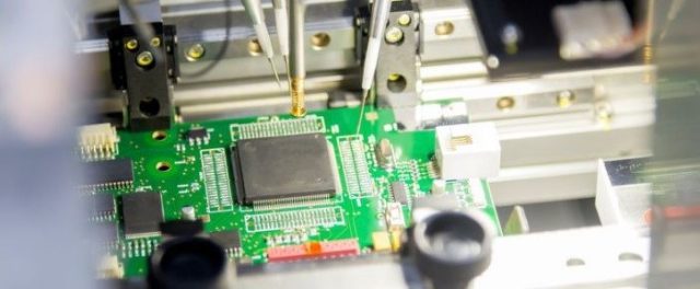
Manufacturing Precision for mmWave PCBs
mmWave performance depends heavily on manufacturing accuracy. Key factors include:
-
Tight control of trace width and spacing
-
Smooth copper surfaces to reduce conductor loss
-
Precise lamination and drilling processes
Experienced manufacturing is essential for consistent mmWave performance.
Testing and Verification of 5G mmWave PCBs
Validation is critical at mmWave frequencies. 5G mmWave PCBs require:
-
Impedance and insertion loss testing
-
Phase and S-parameter verification
-
RF performance consistency checks
Proper testing ensures reliable system operation.
Typical Applications of 5G mmWave PCBs
5G mmWave PCBs are widely used in:
-
5G base stations and small cells
-
mmWave antenna modules
-
High-speed backhaul systems
-
Advanced wireless test equipment
Each application demands low loss and high stability.
Choosing a 5G mmWave PCB Manufacturing Partner
When selecting a 5G mmWave PCB manufacturer, consider:
-
Experience with mmWave frequency designs
-
Capability with low-loss RF materials
-
Precision manufacturing and RF testing
-
Engineering support for antenna and RF integration
The right partner is critical for mmWave success.
Conclusion
The 5G mmWave PCB is a foundational component of next-generation wireless systems. By combining low-loss materials, precise impedance control, antenna-aware design, and high-precision manufacturing, a well-designed 5G mmWave PCB enables reliable, high-speed, and scalable mmWave communication.
Partnering with an experienced 5G mmWave PCB supplier ensures consistent performance from prototype to mass production.
