WiFi PCB Design Guide for High-Speed Connectivity
Introduction
WiFi connectivity is everywhere—from mobile devices to smart home systems and industrial machinery. At the heart of all these wireless systems lies the WiFi PCB, a specialized circuit board engineered to process, transmit, and receive high-frequency wireless signals.
This guide explores the structure, design principles, materials, RF layout challenges, and next-generation requirements for WiFi 6, WiFi 7, and 5G-enabled PCB designs.
1. What Is a WiFi PCB?
A WiFi PCB is the hardware platform enabling wireless communication between devices and WiFi access points. It integrates:
-
RF circuitry
-
WiFi chipsets
-
Antennas
-
Microcontrollers
-
Matching networks
-
Power management blocks
WiFi PCBs operate on 2.4 GHz, 5 GHz, and now 6 GHz (WiFi 6E/7) frequency bands, providing high-speed, high-capacity, and low-latency wireless communication.
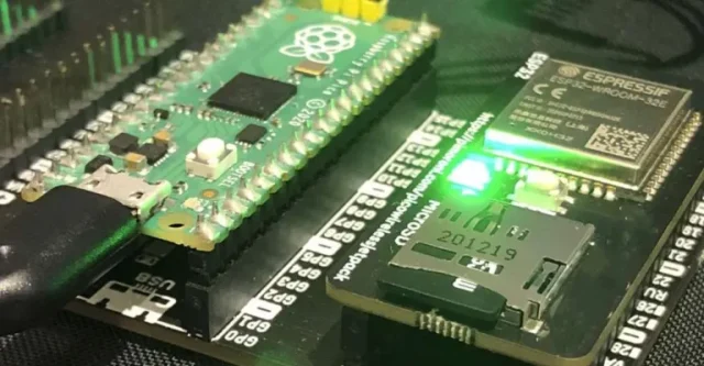
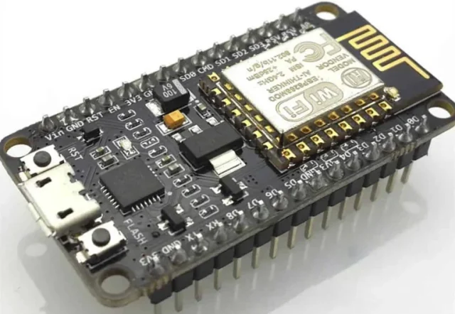
2. Core Components of a WiFi PCB Module
● Microcontroller (MCU)
Acts as the processing brain, running firmware and managing system control.
● WiFi Chipset (Baseband + RF Front End)
-
Baseband handles modulation/demodulation and data encoding
-
RF front-end manages transmission and reception
● PAs and LNAs
-
Power Amplifier (PA): Boosts transmit power
-
Low-Noise Amplifier (LNA): Enhances weak incoming signals
● RF Matching Network
Ensures 50-ohm impedance matching between RF stages and antenna.
● Filters & Oscillators
Stabilize frequency, remove unwanted harmonics, enhance signal cleanliness.
● Flash Memory
Stores firmware, calibration parameters, and configuration data.
● Interfaces (SPI / SDIO / USB / PCIe)
Used for high-speed data exchange with host systems.
3. WiFi PCB Design Guidelines
3.1 Component Placement
-
Keep RF chipset close to the antenna
-
Isolate noisy switching power circuits from RF blocks
-
Position decoupling capacitors as close as possible to IC pins
3.2 Impedance Control & Signal Integrity
-
50-ohm single-ended / 100-ohm differential routing is essential
-
Maintain a solid, continuous ground plane
-
Avoid sharp 90° routing corners
3.3 Power Integrity
-
Use LC filters, ferrite beads, and LDO regulators
-
Apply multi-stage decoupling (0.1uF + 1uF + 10uF)
-
Minimize noise coupling into RF sections
4. WiFi PCB Antenna Design
Common Antenna Types
-
Dipole Antenna – for routers and consumer electronics
-
Patch Antenna – compact IoT devices
-
Monopole Antenna – handheld devices
-
PCB Antenna – cost-efficient, space-saving designs
Placement Guidelines
-
Place antenna at the board edge
-
Keep away from large ground planes and metal structures
-
Maintain a clear keep-out zone on all layers
Antenna Feed & Matching
-
Use 50-ohm feed lines
-
Include π-matching networks for tuning
-
Ensure antenna tuning after final enclosure assembly
Why Dk and Df Are Essential for Superior Wireless Performance
-
Lower Df = Less signal attenuation
-
Stable Dk = Accurate impedance control
6. WiFi PCB Layout Considerations

Routing
-
Avoid long RF traces
-
Keep RF/digital separated
-
Use short via transitions
Ground & Shielding
-
Use ground stitching vias around RF zones
-
Maintain uninterrupted reference planes
Thermal Management
-
Use thermal vias below PA chips
-
Apply copper pours around hot zones
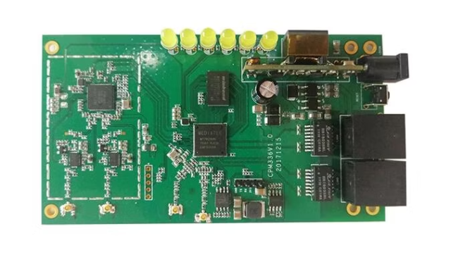
7. Types of WiFi PCBs
-
Single-Layer – small IoT devices
-
Multilayer – routers, laptops, advanced modules
-
Flexible PCB – wearables
-
Rigid-Flex PCB – automotive, medical equipment
8. Applications
-
Consumer electronics
-
Smart home devices
-
Medical monitoring systems
-
Automotive infotainment / ADAS
-
Industrial automation and robotics
9. Trends in WiFi PCB Design
-
WiFi 6 / WiFi 6E / WiFi 7 high-speed PCB
-
WiFi + 5G coexistence architectures
-
Advanced materials for low-loss RF
-
Eco-friendly PCB manufacturing
Conclusion
Designing a high-performance WiFi PCB requires expertise in RF engineering, materials science, signal integrity, and power management. As technologies like WiFi 7 and 5G push wireless performance limits, modern PCB designs must adapt with precision layout, advanced laminates, optimized antennas, and robust EMI strategies.
If you need professional WiFi PCB design & manufacturing, our engineering team can assist with RF simulation, controlled impedance stackup, antenna tuning, and full PCBA services.
