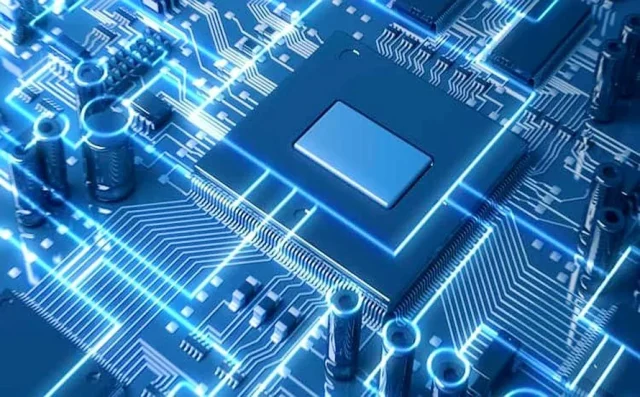
A High Speed PCB forms the electrical backbone of every modern digital communication system, from multi-gigabit SerDes channels to DDR memory interfaces and high-frequency RF-digital mixed platforms. As data rates continue pushing beyond 10 Gbps, 25 Gbps, and even 56–112 Gbps PAM-4, the engineering demands on a High Speed PCB become far more stringent. Signal integrity, loss control, impedance stability, and reference-plane design determine whether a system meets timing and eye-diagram requirements.
At these elevated data rates, a High Speed PCB behaves as a transmission line system rather than a simple interconnect. Dielectric properties—Dk uniformity, low Df, and frequency-dependent dispersion—define how much high-frequency energy can propagate without distortion. High-performance laminates such as Megtron 6, TU-872, Tachyon 100G, or Rogers hybrid builds enable a High Speed PCB to maintain low insertion loss, reduce phase skew, and support multi-gigabit differential signaling across long routing distances.
Stackup engineering is foundational for any High Speed PCB. Designers must pair differential pairs with stable reference planes, minimize dielectric thickness variation, and enforce tight copper roughness control. Surface roughness dramatically influences high-frequency conductor loss; smoother copper creates flatter loss curves, enabling a High Speed PCB to carry higher-order harmonics essential for eye-opening performance. Manufacturing tolerances—etch accuracy, dielectric spacing, via stub length—can shift impedance by several ohms if not precisely controlled.
Via design plays an equally critical role. In a High Speed PCB, poorly managed via stubs introduce resonances that destroy high-frequency energy and collapse link margins. Back-drilling or laser-drilled micro-vias effectively eliminate parasitic resonances, ensuring clean SerDes transitions across layers. For extremely dense high-speed channels, HDI techniques allow designers to shorten return paths, reduce inductance, and maintain controlled impedance throughout the transition.
Crosstalk management becomes a primary constraint. High-speed differential pairs on a High Speed PCB must follow strict spacing rules, maintain consistent coupling, and avoid discontinuities that cause mode conversion. Properly engineered ground stitching, via-fencing, and reference-plane continuity help isolate sensitive lanes, reducing near-end and far-end crosstalk while maintaining channel performance even in complex multi-layer environments.
Power integrity is inseparable from signal integrity in a High Speed PCB. High-speed ICs require extremely low PDN impedance and ultra-fast transient response. Plane resonance suppression, strategic decoupling placement, and optimized PDN stackups prevent excessive supply noise from coupling into high-speed channels. A PDN that is not properly engineered introduces jitter, eye-closure, and link instability, even if the routing is perfectly executed.
KKPCB’s manufacturing capabilities ensure that every High Speed PCB meets the demanding tolerances required for cutting-edge digital systems. Controlled-impedance fabrication, low-roughness copper, advanced HDI processes, back-drilling accuracy, and high-frequency material handling all contribute to repeatable high-speed performance. High-speed testing—TDR, S-parameter characterization, and impedance validation—further guarantee compliance with customer signal-integrity expectations.

As digital systems continue shifting into higher data-rate generations, the High Speed PCB becomes the deciding factor for performance, system reliability, and scalability. Through advanced materials, carefully engineered stackups, and precise fabrication technologies, a High Speed PCB provides the low-loss, low-jitter, and high-fidelity transmission environment necessary for next-generation computing, networking, AI acceleration, and communication equipment.
