
With the continuous development of electronic products toward miniaturization, higher performance, and increased reliability, traditional PCB manufacturing processes are often insufficient to meet the requirements of advanced applications.
Modern electronic systems such as 5G communication equipment, automotive electronics, medical devices, aerospace systems, semiconductor test equipment, and industrial automation products require PCBs with improved electrical performance, mechanical reliability, thermal management capability, and higher manufacturing precision.
To achieve these requirements, PCB manufacturers use various special processing technologies during fabrication. These processes enhance specific PCB characteristics, including:
- High-density interconnection capability
- Signal integrity performance
- Thermal conductivity
- Mechanical reliability
- Surface quality
- Long-term stability
This article introduces common special PCB processing technologies and their applications.
1. HDI PCB Manufacturing Technology
1.1 Overview of HDI Technology
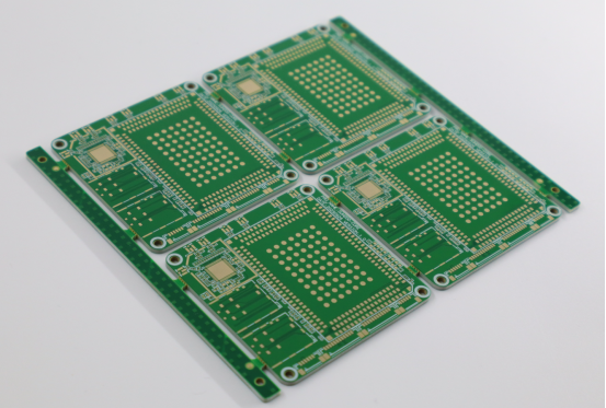
High-Density Interconnect (HDI) is one of the most important advanced PCB manufacturing technologies.
Unlike conventional PCBs that mainly rely on mechanical through holes, HDI uses:
- Laser-drilled microvias
- Fine line routing
- Thin dielectric layers
- Sequential lamination processes
to achieve higher wiring density.
1.2 Advantages of HDI Processing
HDI technology provides:
Higher Routing Density
Smaller vias and finer traces allow more circuits to be placed in limited space.
Better Electrical Performance
Shorter interconnection paths reduce:
- Signal delay
- Parasitic effects
- Signal loss
Smaller Product Size
HDI supports compact designs for:
- Smartphones
- Wearable devices
- Medical electronics
- Portable equipment
1.3 Common HDI Applications
- Mobile communication devices
- High-speed computing systems
- Semiconductor test boards
- Automotive electronic modules
2. Laser Drilling Technology
2.1 What Is Laser Drilling?
Laser drilling uses a focused laser beam to create microvias with extremely small diameters.
Compared with mechanical drilling, laser drilling enables:
- Smaller hole sizes
- Higher precision
- Better suitability for fine-pitch designs
2.2 Advantages of Laser Drilling
Laser drilling improves:
- PCB miniaturization
- Layer interconnection density
- Signal transmission performance
Typical applications include:
- HDI PCBs
- IC substrate-like PCBs
- High-density consumer electronics
3. Copper-Filled Via Technology
3.1 Overview
Copper-filled vias are created by filling vias with electroplated copper instead of leaving hollow spaces.
This process is widely used in:
- Via-in-pad designs
- HDI boards
- High-current applications
3.2 Advantages
Improved Thermal Performance
Solid copper vias provide efficient heat transfer paths.
Useful for:
- Power devices
- LED boards
- High-performance processors
Better Mechanical Reliability
Copper-filled vias improve resistance against:
- Thermal cycling stress
- Via cracking
- Mechanical fatigue
Better SMT Assembly Performance
Via filling prevents:
- Solder flowing into holes
- Solder joint voids
- Assembly defects
4. Controlled Impedance Processing
4.1 Importance of Impedance Control
For high-speed and RF circuits, PCB traces act as transmission lines.
Uncontrolled impedance may cause:
- Signal reflection
- Data errors
- Increased electromagnetic radiation
4.2 Impedance Control Methods
PCB manufacturers control impedance through:
- Precise stackup design
- Dielectric thickness control
- Copper thickness control
- Trace width adjustment
Common impedance requirements include:
- 50 Ω single-ended impedance
- 90 Ω differential impedance
- 100 Ω differential impedance
4.3 Applications
Used in:
- RF PCB
- 5G communication equipment
- High-speed servers
- Automotive radar systems
5. Surface Treatment Technology
Surface finishing protects exposed copper and improves solderability.
Common special surface treatments include:
5.1 ENIG (Electroless Nickel Immersion Gold)
Advantages:
- Flat surface
- Good solderability
- Suitable for fine-pitch components
Applications:
- HDI PCB
- BGA assembly
- High-reliability electronics
5.2 ENEPIG
ENEPIG adds a palladium layer between nickel and gold.
Advantages:
- Improved corrosion resistance
- Better wire bonding capability
- Higher reliability
Applications:
- Semiconductor packaging
- Medical electronics
- Aerospace electronics
5.3 Immersion Silver
Advantages:
- Good electrical performance
- Suitable for high-frequency applications
Considerations:
- Requires proper storage protection
6. Back Drilling Technology
6.1 What Is Back Drilling?
Back drilling removes the unused portion of a plated through hole that extends beyond the required connection layer.
This reduces the unwanted via stub.
6.2 Advantages
Back drilling improves:
- Signal integrity
- High-speed transmission quality
- Reduced resonance effects
6.3 Applications
Commonly used in:
- High-speed servers
- Data communication equipment
- 5G infrastructure
7. Embedded Component Technology
7.1 Overview
Embedded component technology places certain electronic components inside the PCB structure.
Examples:
- Resistors
- Capacitors
- Passive components
7.2 Advantages
Benefits include:
- Reduced PCB size
- Shorter electrical paths
- Improved signal performance
Applications:
- High-density modules
- Miniaturized electronics
8. Heavy Copper PCB Processing
8.1 Overview
Heavy copper PCBs use thicker copper layers to support higher current requirements.
Typical applications include:
- Power supplies
- Motor controllers
- Battery systems
8.2 Advantages
Heavy copper provides:
- Higher current carrying capability
- Better heat dissipation
- Improved mechanical strength
8.3 Manufacturing Challenges
Special control is required for:
- Copper plating uniformity
- Etching accuracy
- Thermal stress management
9. Selective Gold Plating Technology
9.1 Overview
Selective gold plating applies gold only to specific areas requiring enhanced contact performance.
Common areas include:
- Edge connectors
- Contact fingers
- Key interfaces
9.2 Advantages
Provides:
- Better wear resistance
- Lower contact resistance
- Improved connection reliability
Applications:
- Industrial control equipment
- Communication systems
- Testing equipment
10. Flexible and Rigid-Flex PCB Processing
10.1 Flexible PCB Processing
Flexible PCB manufacturing uses materials such as:
- Polyimide films
- Flexible copper laminates
Special processes include:
- Coverlay processing
- Flexible layer lamination
- Precision cutting
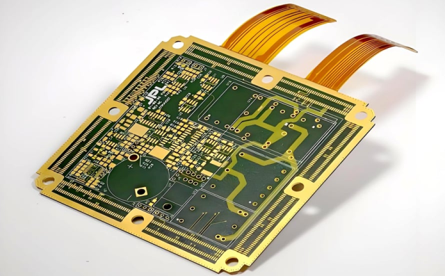
10.2 Rigid-Flex PCB Processing
Rigid-flex PCBs combine:
- Rigid PCB structures
- Flexible circuit sections
Special manufacturing requirements include:
- Controlled lamination
- Flexible area protection
- Precise layer alignment
Applications:
- Medical devices
- Aerospace electronics
- Wearable products
11. Thermal Management Processing
For high-power electronic systems, PCB manufacturers may use special thermal technologies.
Examples include:
Thermal Vias
Copper-filled thermal vias transfer heat from components to internal copper layers.
Metal Core PCB
Metal substrates such as:
- Aluminum
- Copper
provide improved heat dissipation.
Applications:
- LED lighting
- Power electronics
- Motor control systems
12. PCB Surface and Appearance Processing
Special appearance processes may include:
- Carbon ink printing
- Peelable mask processing
- Selective solder mask opening
- Special marking processes
These are used for:
- Electrical contacts
- Temporary protection
- Special assembly requirements
13. Inspection and Quality Control for Special Processes
Advanced PCB processing requires strict quality verification.
Common inspection methods include:
AOI Inspection
Checks:
- Circuit defects
- Line width issues
- Pattern accuracy
X-Ray Inspection
Used for:
- Via filling quality
- Internal structures
- Hidden defects
Cross-Section Analysis
Evaluates:
- Copper thickness
- Plating quality
- Layer bonding
Electrical Testing
Includes:
- Flying probe testing
- Fixture testing
- Impedance testing
14. Importance of DFM Review in Special PCB Processing
Special PCB technologies often involve complex manufacturing requirements.
Early Design for Manufacturability (DFM) analysis helps evaluate:
- Via structures
- Stackup feasibility
- Minimum trace spacing
- Material selection
- Manufacturing tolerance
A proper DFM review reduces:
- Production risks
- Prototype failures
- Manufacturing delays
and improves:
- First-pass yield
- Production consistency
- Product reliability
Conclusion
Special PCB processing technologies provide essential solutions for modern electronic products requiring higher performance, smaller size, and greater reliability.
Technologies such as:
- HDI manufacturing
- Laser drilling
- Copper-filled vias
- Controlled impedance processing
- Advanced surface finishing
- Back drilling
- Heavy copper fabrication
- Rigid-flex processing
enable PCBs to meet the demanding requirements of industries including communication, automotive, medical, industrial automation, and semiconductor testing.
As electronic systems continue evolving toward higher speeds and greater integration, advanced PCB manufacturing processes will remain a key factor in achieving reliable and high-performance electronic products.
