
Engineering intent. High-power RF modules combine heat, current, and microwave loss in a small area. This article presents a practical workflow for using an RO3003 PCB as part of a thermal-aware RF module. It is a design guide, not a customer case study or a measured KKPCB result.
RO3003 is a ceramic-filled PTFE laminate in the Rogers RO3000 family. Supplier data should be used with the stated test conditions, while the finished stackup, copper, interfaces, and enclosure remain design variables. Thermal decisions should therefore be connected to the released construction rather than to a material name alone.
Why RF thermal design starts with the stackup
At high power, heat leaves the amplifier through component leads, copper planes, vias, the board edge, and the mechanical interface. The same layers also carry the RF return current. A thermal change that improves spreading can alter reference-plane continuity, line width, or the launch geometry. The stackup is consequently a coupled electrical and thermal decision.
Begin by identifying the dominant heat sources, their duty cycle, the allowable junction temperature, and the available heat path into the chassis or heatsink. Separate a supplier typical material value from a thermal limit validated for the assembled module.
Map the heat path before choosing copper
A fabrication-ready RO3003 PCB design should show the heat source, spreading copper, thermal vias, plane transitions, and mechanical contact in one cross-section. This makes it easier to spot an insulating layer, an unconnected copper island, or a via field that conflicts with a launch.
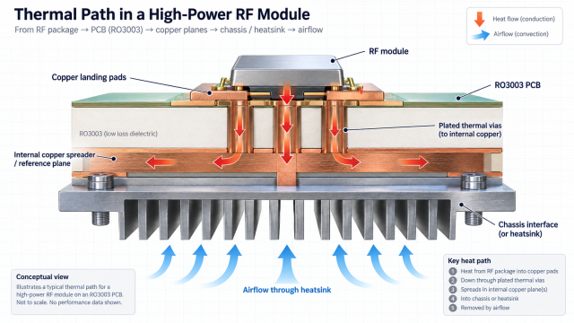
| Thermal region | Design question | Release evidence |
|---|---|---|
| Device pad | Where does heat enter the copper? | Footprint pad, voiding note, and solder process. |
| Spreader plane | Which copper area carries heat laterally? | Layer map, copper balance, and keepout review. |
| Via field | Can heat cross the dielectric without disrupting RF current? | Via diameter, pitch, fill or cap note, and return-path check. |
| Mechanical boundary | Where does heat leave the board? | Interface material, flatness target, and chassis datum. |
Keep the same stackup inputs in the thermal model, field solver, PCB layout library, and fabrication drawing. If a press construction changes, rerun both the impedance and thermal assumptions.
Use copper and vias without breaking the RF path
Thermal copper under active devices
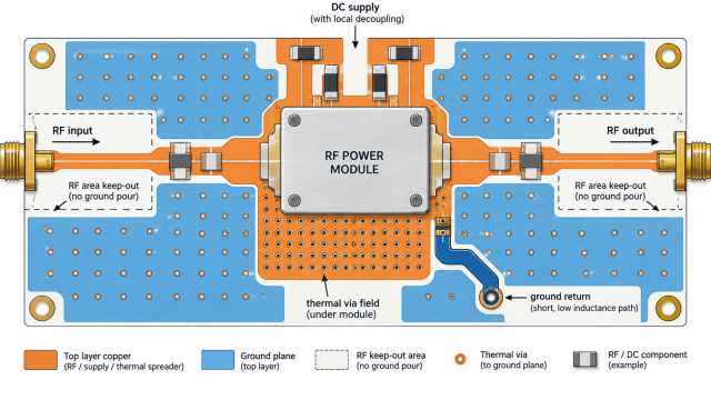
Large copper regions can reduce spreading resistance, but they can also increase parasitic capacitance or disturb a microstrip launch. Define the device pad, solder mask opening, and nearby ground boundary together. Avoid claiming a universal copper area or temperature drop without a validated model.
Via arrays and return-current continuity
Thermal vias can transfer heat toward a plane or chassis interface. At the same time, ground vias around an RF trace contain the return field. A RF PCB capability review should check via pitch, drill tolerance, antipad clearance, and whether the thermal array creates a slot in the reference plane.
Use a compact via transition where the RF path changes layers. Remove unused barrels only when the fabrication process and reliability requirements allow it. The finished via structure must be reviewed as an electrical discontinuity and a thermal conductor.
Co-design the enclosure and the board
The board-to-chassis interface often controls the real thermal bottleneck. Specify the contact area, interface material, pressure, flatness, and screw pattern at the same time as the PCB materials selection. A supplier laminate value is not a substitute for a module-level thermal boundary condition.
Keep high-current digital converters outside the sensitive RF zone where possible. Route their return paths directly to the power entry and prevent them from sharing narrow necks with the amplifier return. If the module uses a shield, model the shield wall and its attachment points before freezing the component placement.
Thermal verification without overstating the result
A conceptual design should define target temperatures and measurement locations, not invent measured results. Establish a baseline model with the supplier material inputs, copper thickness, device power, ambient condition, and interface assumptions. Then compare the model with a prototype using documented fixtures.
| Review stage | Check | Decision |
|---|---|---|
| Pre-layout | Device power map and proposed heat path | Approve the thermal architecture. |
| Layout | RF return paths, via fields, and copper balance | Approve the coupled geometry. |
| Fabrication | Finished dielectric, copper, drilling, and interface notes | Release the build definition. |
| Prototype | Fixture temperature and RF checks at defined power | Compare with targets; do not generalize beyond the test setup. |
KKPCB can review the PCB manufacturing services notes for drilling, lamination, copper treatment, and inspection. The purpose is to preserve the intended heat and RF paths through fabrication, not to promise a universal thermal performance.
For the design record, link the thermal assumptions to the RO3003 PCB stackup and list every interface that can change the result.
Release checklist for a high-power RF module
- Confirm the device power map and operating duty cycle.
- Show the thermal path from pad to plane, via field, and chassis.
- Check that thermal vias do not interrupt the RF reference plane.
- Carry copper thickness, finished dielectric, and interface assumptions into the model.
- Define target values separately from typical material values and measured prototype data.
Before a revision is frozen, verify that the RO3003 PCB layout and the mechanical interface still match the thermal model. If the assembly changes, reassess the heat path instead of reusing an earlier conclusion.
Where a change affects production, update the RO3003 PCB fabrication notes and the inspection plan. This keeps a high-power RF design traceable from concept to build.
Sources: Rogers RO3000 Series Laminates product information; Rogers RO3000 laminate data sheet for RO3003; Rogers fabrication guidelines for RO3000 and RO3200 series high-frequency circuit materials. Supplier values are used under their stated conditions and are not finished-board measurements.
For RF module sourcing, review KKPCB’s RF PCB manufacturing route before freezing the thermal interface.
