As wireless communication systems and RF electronics continue to move toward higher frequencies and higher integration, the demand for stable and low-loss PCB materials is increasing rapidly. From 5G base stations and WiFi modules to GPS devices, radar sensors, and high-performance RF front-end circuits, signal transmission quality is now one of the most critical design factors.
In these applications, the PCB is no longer just a mechanical carrier for components—it becomes part of the RF circuit. The dielectric material, stack-up structure, trace geometry, and via transitions all affect insertion loss, return loss, impedance stability, and overall high frequency signal integrity.
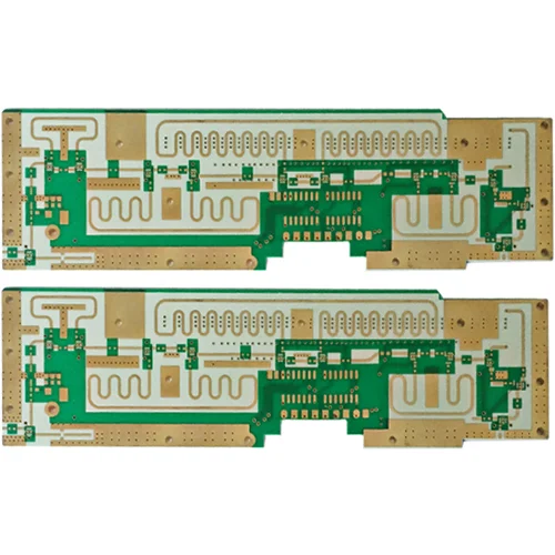
RO4003C PCB is one of the most widely used Rogers PCB material options for high frequency PCB designs. It offers an excellent balance of performance, manufacturability, and cost, making it a preferred solution for controlled impedance RF routing and stable GHz-level signal transmission.
What Is an RO4003C PCB?
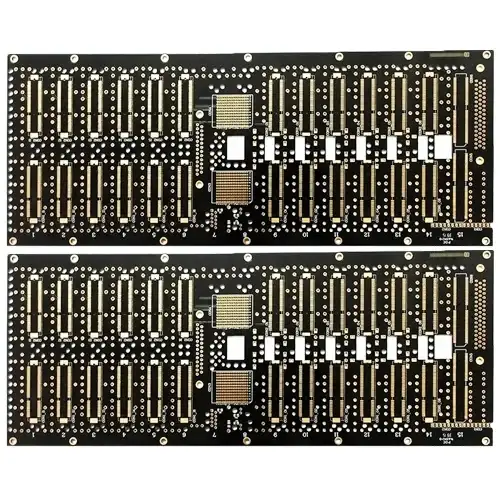
An RO4003C PCB is a printed circuit board manufactured using Rogers RO4003C laminate, which is a hydrocarbon ceramic high-frequency material developed for RF and microwave applications. RO4003C is designed to provide stable dielectric performance and lower signal loss compared to standard FR-4, especially when routing RF traces and high frequency signal lines.
RO4003C PCBs are commonly used for:
-
RF trace PCB routing and transmission line design
-
Controlled impedance PCB applications (50Ω microstrip, stripline, etc.)
-
Antenna feed networks and RF connector launches
-
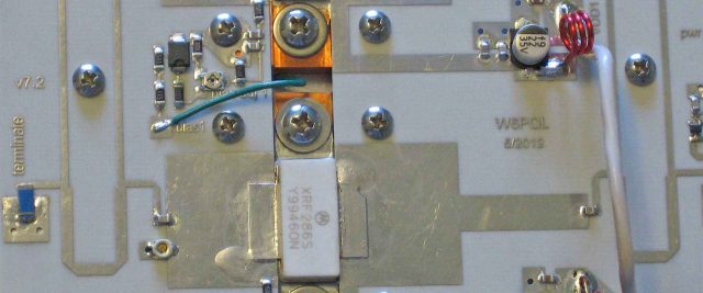
RF front-end modules such as filters, couplers, LNAs, and PAs
-
Wireless communication, radar, and high frequency signal circuits
For many engineers, RO4003C PCB is a practical choice because it offers high-frequency stability while remaining easier to fabricate than some PTFE-based materials.
Why Choose RO4003C PCB for High Frequency Designs?
1. Controlled Impedance Performance for RF Signal Routing
Controlled impedance is a core requirement in most RF and high frequency signal PCB designs. At GHz frequencies, traces behave like transmission lines, meaning impedance mismatch can cause reflections, waveform distortion, and power loss.
RO4003C PCB is widely selected because it supports:
-
Stable 50Ω microstrip and stripline routing
-
Reliable impedance control across production batches
-
Improved return loss performance
-
Better consistency for RF tuning and matching networks
With a well-designed stack-up and proper manufacturing control, RO4003C PCB helps maintain stable impedance for high-frequency signal transmission.
2. Low Loss for Better Insertion Loss Performance
As frequency increases, signal loss becomes a major challenge. Loss comes from both dielectric absorption and conductor effects. Excessive loss reduces signal strength and impacts system sensitivity, especially in RF receivers and long transmission lines.
RO4003C PCB helps reduce insertion loss by offering lower dielectric loss compared to standard FR-4. This improves:
-
RF efficiency and signal amplitude
-
Receiver sensitivity and link performance
-
Overall stability of high frequency signal PCB designs
For many high frequency PCB applications, RO4003C provides a strong balance between performance and cost.
3. Stable Electrical Properties for Reliable High Frequency Signal Integrity
High frequency signal integrity depends on the stability of the PCB material. If dielectric constant varies significantly with frequency or temperature, the impedance and phase response can shift, leading to inconsistent RF behavior.
RO4003C PCB supports stable signal integrity by providing:
-
Consistent dielectric behavior for predictable RF routing
-
Better repeatability for production manufacturing
-
Improved reliability in high frequency signal environments
This makes RO4003C PCB suitable for RF designs where consistent performance is required across multiple units.
RO4003C PCB vs FR-4 PCB: Key Differences
FR-4 is widely used for general electronics, but it often becomes a limitation for high-frequency circuits due to higher loss and less stable dielectric characteristics.
Compared with FR-4, RO4003C PCB provides:
-
Lower loss for RF and microwave signal routing
-
More stable impedance control for transmission lines
-
Better performance at GHz frequencies
-
Improved repeatability for RF signal applications
For designs involving antennas, RF modules, or microwave circuits, RO4003C PCB can significantly improve performance compared to standard FR-4.
Typical Applications of RO4003C PCB
RO4003C PCB is widely used in high-frequency and RF industries, including:
-
5G communication equipment and wireless infrastructure
-
WiFi and Bluetooth modules
-
GPS positioning and navigation systems
-
Radar sensors and automotive radar electronics
-
RF front-end circuits: filters, couplers, LNAs, PAs
-
Antenna feed networks and matching circuits
-
Wireless IoT communication products
Because RO4003C supports controlled impedance and low-loss RF routing, it is commonly used in both commercial and industrial RF applications.
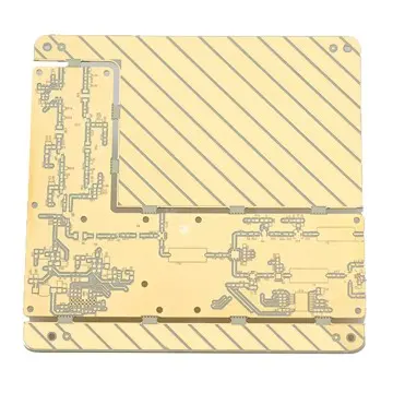
RO4003C PCB Stack-Up and RF Trace Design Considerations
To maximize RO4003C PCB performance, designers should pay close attention to stack-up planning and RF trace routing structures.
Microstrip vs Stripline in RO4003C PCB
RO4003C PCB routing commonly uses two transmission line structures:
Microstrip (outer layer trace + reference plane)
-
Easy to tune and measure
-
Common for antenna feeds and RF components
-
Practical for many RF trace PCB designs
Stripline (inner layer trace between planes)
-
Better shielding and lower radiation
-
Improved isolation in dense layouts
-
Often used in multilayer high frequency PCB designs
Choosing the right structure depends on EMI control requirements, routing density, and signal frequency.
Grounding and Return Path Design
A stable ground reference is critical for RF trace routing. Poor grounding can cause return path discontinuities, leading to increased noise, EMI, and unstable impedance.
RO4003C PCB designs typically include:
-
Solid and continuous ground planes
-
Ground via stitching near RF traces
-
Ground fences for isolation and EMI control
-
Careful avoidance of routing across split planes
These practices improve RF stability and reduce interference.
RO4003C PCB Manufacturing Requirements
To ensure consistent RF performance, RO4003C PCB manufacturing must maintain strict control over key processes.
1. Stack-Up Accuracy and Lamination Control
Trace impedance depends on dielectric thickness and layer spacing. Accurate lamination ensures stable controlled impedance performance.
2. Trace Width and Etching Precision
Small variations in RF trace width can cause impedance deviation. High precision etching control is essential for RO4003C PCB fabrication.
3. Controlled Impedance Testing
For RF and high frequency signal PCBs, impedance verification is often required to confirm 50Ω or other specified impedance values.
4. Via Reliability and RF Transition Control
Vias can introduce discontinuities in high-frequency routing. Proper drilling, plating, and via design reduce signal degradation and improve performance.
5. Surface Finish Selection
Surface finish impacts both solderability and high-frequency loss. A suitable finish supports stable RF performance during assembly and long-term use.
Best Practices for RO4003C PCB RF Layout
To achieve the best performance from RO4003C PCB designs, engineers often follow these RF layout recommendations:
-
Keep RF traces short and direct
-
Avoid sharp corners; use smooth bends or arcs
-
Maintain consistent trace width and spacing
-
Minimize via transitions and reduce via stubs
-
Keep RF traces away from switching power noise
-
Use proper RF connector launch design
-
Add ground via stitching near RF traces and connectors
-
Ensure continuous reference planes under RF traces
These design practices help improve insertion loss, reduce reflections, and maintain stable controlled impedance.
Conclusion: RO4003C PCB for Reliable High Frequency Performance
An RO4003C PCB is a proven and widely used solution for high frequency PCB designs requiring controlled impedance, low insertion loss, and stable RF signal integrity. As part of the Rogers PCB material family, RO4003C supports reliable GHz-level signal routing for applications such as 5G communication, WiFi modules, GPS systems, radar sensors, and RF front-end circuits.
By combining proper RF stack-up design, controlled impedance routing, and precision RO4003C PCB manufacturing, engineers can achieve stable performance and scalable production results.
If your project requires a RO4003C Rogers PCB, KKPCB can support you with engineering review, impedance control, and high-reliability high frequency PCB fabrication.
