What Is an RO4003C PCB?
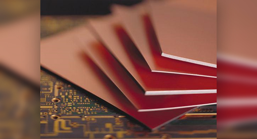
An RO4003C PCB is a high-frequency printed circuit board manufactured using Rogers RO4003C laminate, a popular RF material designed for high-frequency and microwave applications. Compared with standard FR-4, RO4003C offers lower dielectric loss, more stable dielectric constant (Dk), and better performance for controlled impedance routing.
Because of its excellent electrical stability and cost-effective performance, RO4003C PCB is widely used in RF trace PCB, high frequency signal PCB, wireless communication PCB, and 5G RF module PCB designs.
Why RO4003C PCB Is Widely Used in RF Designs
RO4003C is one of the most commonly selected Rogers materials for RF and high-frequency circuits because it provides a strong balance of:
-
High-frequency performance
-
Stable controlled impedance behavior
-
Manufacturability similar to FR-4 processing
-
Good reliability for multilayer PCB production
-
Cost efficiency compared with ultra-low-loss PTFE materials
For many RF and microwave products, an RO4003C PCB is the ideal choice to improve performance while controlling overall cost.
Key Advantages of RO4003C PCB
1. Low Loss Performance for High Frequency Signals
An RO4003C PCB is designed to reduce signal attenuation and insertion loss, improving:
-
RF transmission efficiency
-
Signal integrity for high-frequency signals
-
Overall system stability at GHz-level frequencies
Low loss PCB performance is essential for 5G, WiFi, GPS, and RF module designs.
2. Stable Dielectric Constant (Dk) for Impedance Control
RO4003C laminate provides stable Dk behavior, which helps maintain accurate impedance control for:
-
50Ω RF traces
-
75Ω RF transmission lines
-
100Ω differential pair PCB routing
Stable impedance control is critical to reduce reflection, improve return loss, and ensure consistent RF performance.
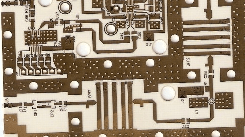
3. Excellent Controlled Impedance PCB Compatibility
RO4003C PCB manufacturing supports controlled impedance routing structures such as:
-
Microstrip PCB
-
Stripline PCB
-
Coplanar waveguide (CPW) PCB
These structures are commonly used in RF trace PCB and high frequency signal PCB layouts.
4. Strong Reliability and Dimensional Stability
RO4003C PCB designs benefit from good mechanical stability, helping reduce:
-
Warpage during lamination
-
Layer misalignment in multilayer boards
-
Reliability risks under thermal stress
This makes RO4003C PCB suitable for automotive, industrial, and communication electronics.
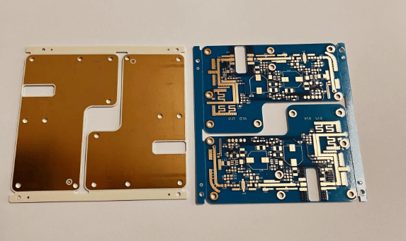
5. Hybrid PCB Stack-Up Options (RO4003C + FR-4)
To balance cost and performance, many customers choose hybrid PCB stack-ups combining:
-
RO4003C layers for RF signal paths
-
FR-4 layers for control, power, and digital circuits
Hybrid RO4003C PCB solutions are widely used in compact wireless modules and high-speed communication products.
RO4003C PCB Design Considerations
1. RF Trace Routing and Geometry Control
RO4003C PCB design must follow strict RF routing rules, including:
-
Smooth bends and consistent trace width
-
Avoiding sharp corners and sudden transitions
-
Short RF trace lengths to reduce insertion loss
-
Proper spacing to reduce coupling and crosstalk
These practices help maintain stable RF trace performance.
2. Grounding and Via Stitching for RF Shielding
Good grounding is essential in RO4003C PCB layouts. Recommended techniques include:
-
Solid ground planes under RF traces
-
Via stitching near RF transmission lines
-
Ground fences around sensitive RF sections
-
Clean return paths to minimize loop area
This improves EMI control and RF stability.
3. Connector Launch and Via Transition Optimization
At high frequency, vias and connectors introduce discontinuities. RO4003C PCB designs should focus on:
-
Optimized connector launch geometry
-
Symmetrical via transitions
-
Reduced via stubs and reflection control
-
Backdrill options if required for very high-speed paths
Proper transitions improve insertion loss and return loss performance.
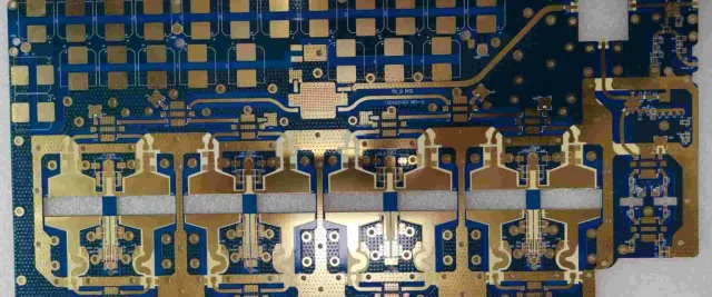
4. Stack-Up Planning for RF and High-Speed Signals
RO4003C PCB stack-up design affects impedance, shielding, and performance. Common approaches include:
-
Microstrip routing on outer layers for RF traces
-
Stripline routing for improved EMI shielding
-
Dedicated ground reference planes for stable return paths
-
Separation of RF and noisy digital sections
Stack-up optimization is critical for controlled impedance PCB manufacturing.
Typical Applications of RO4003C PCB
RO4003C PCBs are widely used in:
-
5G RF modules and small cells
-
WiFi / Bluetooth communication boards
-
GPS receivers and positioning modules
-
RF front-end modules (FEM)
-
Antenna feed networks and matching circuits
-
Automotive radar and ADAS RF boards
-
High-frequency test boards and RF measurement systems
-
Telecom equipment and wireless infrastructure
KKPCB RO4003C PCB Manufacturing Capabilities
KKPCB provides professional RO4003C PCB manufacturing with stable quality control and engineering support, including:
-
Rogers RO4003C PCB fabrication
-
Controlled impedance PCB production and testing
-
Multilayer RO4003C PCB and hybrid stack-up support
-
Fine line PCB manufacturing for dense RF modules
-
HDI PCB and microvia options when required
-
High reliability inspection and process control
-
Prototype to mass production support
We help customers build RO4003C PCBs with stable RF performance, consistent impedance control, and reliable manufacturing quality.
Conclusion
An RO4003C PCB is an excellent solution for RF and high-frequency electronics that require low loss, stable dielectric properties, and controlled impedance routing. With strong manufacturability and reliable performance, RO4003C PCB is widely used in 5G, wireless communication, GPS, antennas, radar, and high-frequency test applications.
KKPCB delivers high-quality RO4003C PCB manufacturing to support advanced RF products with stable performance and high reliability.
