What is an RF Trace PCB?
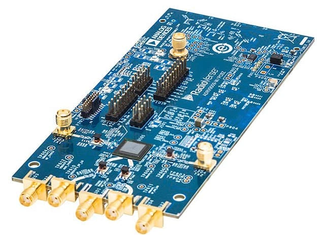
An RF Trace PCB refers to a printed circuit board specifically designed with controlled impedance traces to handle radio frequency (RF) signals. Unlike standard PCB routing, RF traces must maintain consistent electrical characteristics to avoid signal loss, reflection, and distortion.
In RF design, the trace itself becomes part of the circuit—its width, spacing, and layout directly affect performance.
Why RF Trace Design Matters
At high frequencies, even small layout variations can cause major issues:
- Signal reflection due to impedance mismatch
- Increased insertion loss
- Crosstalk between traces
- Electromagnetic interference (EMI)
Key RF Trace Structures
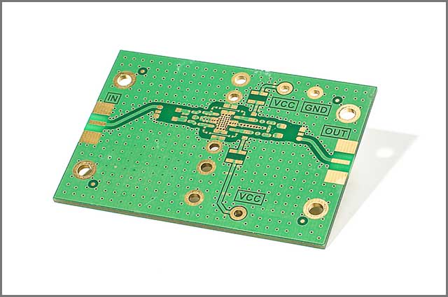
1. Microstrip
- Trace on outer layer with a ground plane below
- Easy to manufacture and tune
- Common in RF PCB design
2. Stripline
- Trace embedded between two ground planes
- Better shielding and lower EMI
- More complex and costly
3. Coplanar Waveguide (CPW)
- Ground planes on the same layer as the trace
- Improved impedance control
- Widely used in compact RF designs
Controlled Impedance Basics
RF traces must be designed with precise impedance, typically:
- 50Ω (most RF systems)
- 75Ω (video and certain communication systems)
Key factors affecting impedance include:
- Trace width
- Substrate thickness
- Dielectric constant (Dk)
- Copper thickness
Impedance Relationship (Simplified)
Z0∝hεr⋅wZ_0 \propto \sqrt{\frac{h}{\varepsilon_r \cdot w}}Z0∝εr⋅wh
Where:
- Z0Z_0Z0 = characteristic impedance
- hhh = substrate height
- www = trace width
- εr\varepsilon_rεr = dielectric constant
Material Selection for RF Trace PCB
Material choice directly impacts signal performance:
1. FR4
- Low cost
- High loss at high frequencies
- Only suitable for low-frequency RF
2. PTFE-Based Materials
- Very low loss
- Ideal for microwave and high-frequency designs
3. High-Frequency Laminates
- Stable dielectric properties
- Used in 5G, radar, and aerospace
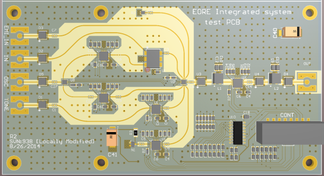
RF Trace Layout Guidelines
1. Keep Trace Length Short
Reduces insertion loss and signal delay.
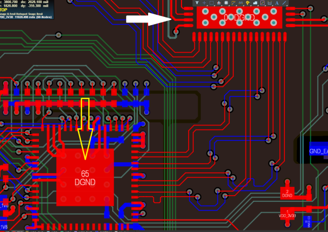
2. Maintain Continuous Ground Plane
Avoid gaps that disrupt return current paths.
3. Avoid Sharp Corners
Use 45° bends or arcs to minimize reflection.
4. Control Trace Spacing
Prevent crosstalk between RF signals.
5. Minimize Vias
Each via introduces impedance discontinuity and signal loss.
Common Design Mistakes
- Ignoring impedance calculation
- Using FR4 for high-frequency designs
- Poor grounding strategy
- Excessive vias in RF paths
- Inconsistent trace width
Applications of RF Trace PCB
1. 5G Communication Systems
High-frequency signal routing for base stations and modules.
2. Radar Systems
Automotive and defense radar circuits.
3. RF Antennas
Precise impedance matching is critical.
4. Satellite Communication
Long-distance signal transmission stability.
5. Wireless Devices
Wi-Fi, Bluetooth, and IoT modules.
Manufacturing Considerations
RF Trace PCB requires tight process control:
- Accurate impedance control
- Consistent dielectric thickness
- Precision etching for trace width
- Stable material properties
When is RF Trace PCB Critical?
You must prioritize RF trace design when:
- Operating frequency > 1 GHz
- Signal integrity is critical
- System involves antennas or RF modules
- High-speed digital behaves like RF
Conclusion
RF Trace PCB design is not just about routing—it is about engineering the signal path. Controlled impedance, proper materials, and optimized layout are essential to ensure reliable high-frequency performance.
Without proper RF trace design, even the best components cannot deliver expected results.
