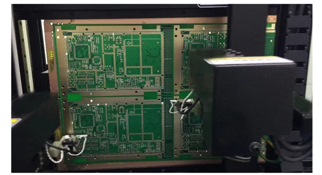
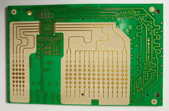
An RF Test PCB is a printed circuit board engineered to support high-frequency testing, characterization, and validation of RF and microwave components. Unlike standard PCBs, RF test boards are optimized for signal integrity, controlled impedance, and minimal insertion loss, ensuring that measurements accurately reflect the performance of devices under test (DUT).
RF test PCBs are widely used in:
-
Semiconductor testing laboratories
-
RF module validation (amplifiers, filters, transceivers)
-
High-frequency communication systems
-
Aerospace and defense electronics
The primary goal is to provide a stable, low-noise environment for precise characterization of RF components and systems.
Design Challenges
Designing RF test PCBs presents several technical challenges:
-
Controlled Impedance: High-frequency signals require precise trace width, spacing, and layer stack-up to prevent reflections and signal loss.
-
Minimizing Crosstalk & EMI: Dense test configurations can induce interference between adjacent test traces and components.
-
High-Frequency Signal Loss: Dielectric and conductor losses can distort measurements, requiring low-loss laminates and optimized trace geometry.
-
Thermal Management: High-frequency operation and extended testing can generate localized heat, affecting material properties and test accuracy.
-
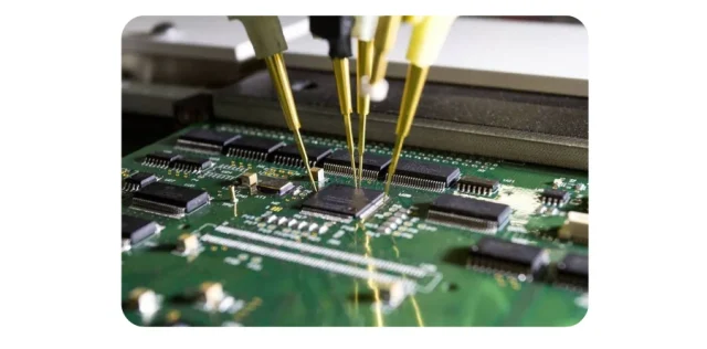
Mechanical Reliability: Frequent insertion and removal of test sockets or connectors necessitate reinforced pads and vias to prevent damage.
Engineering Solutions
To overcome these challenges, engineers implement the following strategies:
-
Controlled Impedance Traces: Microstrip, stripline, and coplanar waveguide designs ensure consistent impedance for accurate measurement.
-
Shielding & Grounding: Guard traces, ground planes, and via fences reduce EMI and maintain signal fidelity.
-
High-Precision Trace Layout: Smooth bends, gradual transitions, and minimal stub lengths prevent reflections and insertion loss.
-
Thermal Vias & Copper Planes: Efficient heat spreading protects substrate integrity during prolonged testing.
-
Socket & Connector Reinforcement: Multiple vias and plated-through holes strengthen critical test points for repeated DUT insertion.
Fabrication & Quality Assurance
RF test PCBs require specialized materials and precise manufacturing processes:
-
Low-Loss Laminates: PTFE-based, Rogers, or ceramic-filled substrates minimize dielectric loss at GHz frequencies.
-
Precision Drilling & Plating: Microvias and through-holes maintain consistent signal paths.
-
Surface Finishes: ENIG, hard-gold, or immersion silver improve durability and measurement reliability.
-
QA Processes:
-
Impedance testing and Vector Network Analysis (VNA) validate trace performance
-
AOI/X-ray inspections ensure via, pad, and layer integrity
-
Thermal cycling verifies board stability under operational conditions
-
KKPCB applies these techniques to deliver RF test PCBs with high measurement fidelity and long-term reliability.
Applications
RF test PCBs are essential in industries requiring precise high-frequency validation:
-
Semiconductor Testing: Characterizing RF ICs, transceivers, and power amplifiers
-
Wireless Communication: Testing antennas, filters, and 5G modules
-
Aerospace & Defense: Radar, satellite, and secure communication component validation
-
High-Frequency Networking Equipment: Router, switch, and signal distribution testing
-
Test & Measurement Laboratories: Spectrum analyzers, vector network analyzers, and RF diagnostic tools
By combining low-loss materials, precise trace design, controlled impedance, and robust QA, KKPCB ensures RF test PCBs deliver accurate, reliable, and repeatable testing environments for high-frequency electronics.
