Why RF IC Testing Is Fundamentally Different
Testing RF integrated circuits is significantly more demanding than standard digital testing. An RF IC Test PCB must handle GHz-level signals, where even small discontinuities can distort measurement results.
Unlike digital systems, RF testing is highly sensitive to:
- Signal loss and phase shift
- Impedance discontinuities
- Parasitic effects from vias and transitions
- Environmental and thermal variations
At high frequencies, the PCB itself becomes part of the measurement system. This means the board must be designed not just for connectivity, but for signal fidelity and measurement accuracy.
Signal Path Engineering
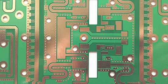
The most critical aspect of an RF IC test PCB is the signal path. Every trace, via, and connector affects performance.
Key design principles include:
- Shortest Possible RF Paths:
Minimize insertion loss and reduce exposure to noise and interference. - Controlled Impedance Transmission Lines:
Microstrip or stripline structures must be precisely designed to maintain impedance consistency. - Minimized Discontinuities:
Transitions between layers, connectors, and components must be optimized to avoid reflections. - Via Optimization:
Use back-drilling or microvias to eliminate via stubs that degrade RF performance. - Grounding Strategy:
Continuous ground planes and via fencing improve return paths and reduce EMI.
In RF testing, even millimeter-level routing differences can impact results.
Accuracy & Calibration
Accurate RF testing requires more than good layout—it depends on calibration and repeatability.
- De-Embedding Techniques:
Used to remove the effect of the PCB and test fixtures from measurement results. - Calibration Structures:
Open, short, load, and thru (OSLT) structures are often integrated into the PCB. - Repeatability:
The PCB must deliver consistent results across multiple test cycles. - Connector Stability:
High-quality RF connectors (e.g., SMA, SMP) are critical for reliable measurements. - Thermal Stability:
Temperature variations can affect dielectric properties and signal behavior.
Without proper calibration, even a well-designed PCB can produce misleading test data.
Materials & Layout Considerations
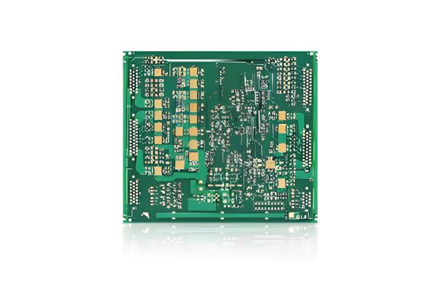
Material selection is crucial for RF IC test PCBs:
- Low-Loss Materials:
PTFE-based or hydrocarbon ceramic laminates reduce dielectric loss at high frequencies. - Stable Dielectric Constant (Dk):
Ensures consistent impedance and phase response. - Low Dissipation Factor (Df):
Minimizes signal attenuation. - Smooth Copper Foil:
Reduces conductor loss caused by surface roughness. - Hybrid Stack-Ups:
Combining RF materials with FR-4 helps optimize cost without sacrificing performance.
Layout must align with material behavior to ensure predictable RF performance.
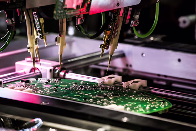
Manufacturing & Validation
RF IC test PCBs require strict fabrication control and advanced validation:
- Tight Tolerances:
Trace width, spacing, and dielectric thickness must be precisely controlled. - Surface Finish Selection:
ENIG or immersion silver is preferred for RF performance. - Advanced Inspection:
- X-ray for internal structures
- AOI for fine features
- Cross-section analysis
- High-Frequency Testing:
- TDR for impedance verification
- VNA for insertion/return loss
- RF calibration validation
At KKPCB, we ensure RF test PCBs meet high-frequency performance standards and measurement accuracy requirements.
Final Thoughts
RF IC Test PCBs are not just test fixtures—they are precision measurement platforms that directly influence the accuracy of RF device characterization.
Success in RF testing depends on:
- Clean signal paths
- Low-loss materials
- Precise impedance control
- Reliable calibration methods
By combining advanced RF design techniques, optimized materials, and strict manufacturing control, KKPCB delivers RF IC Test PCBs that support accurate and repeatable high-frequency testing.
