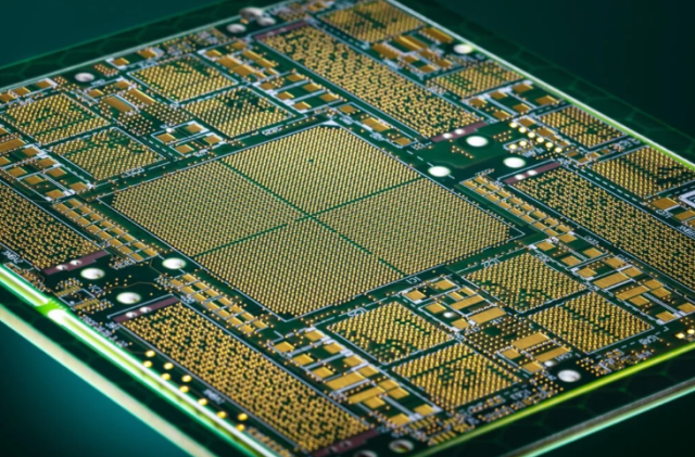
An RF IC Test PCB is a specialized semiconductor test board engineered for validating radio frequency (RF) integrated circuits in Automated Test Equipment (ATE) systems. These test PCBs are used to evaluate critical RF parameters such as gain, noise figure, linearity, phase, and frequency response, ensuring that RF ICs meet strict performance specifications before mass production.
As RF ICs are widely used in 5G communication, IoT devices, automotive radar, satellite systems, and wireless modules, the design and manufacturing of RF IC test PCBs require advanced expertise in high-frequency signal integrity and low-loss PCB technology.
Key Design Requirements of RF IC Test PCBs
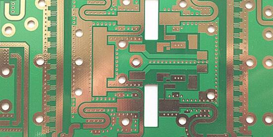
1. Controlled Impedance and RF Signal Integrity
RF IC test PCBs require precise controlled impedance transmission lines to minimize reflection, insertion loss, and phase distortion during high-frequency testing.
2. Low-Loss PCB Materials
To preserve RF signal quality, low-Dk and low-Df laminates such as PTFE or high-frequency Rogers materials are often used in RF IC test PCB construction.
3. Grounding and Shielding Optimization
Proper grounding, via fencing, and shielding techniques reduce electromagnetic interference (EMI) and crosstalk, ensuring accurate RF measurements.
4. Power Integrity and Noise Suppression
RF ICs are sensitive to power noise. Carefully designed power planes, decoupling capacitors, and isolation structures ensure stable and repeatable test conditions.
5. Precision Connector and Socket Integration
Accurate RF testing depends on precise integration of RF connectors, coax interfaces, and test sockets, minimizing signal discontinuities and measurement errors.
Applications of RF IC Test PCBs
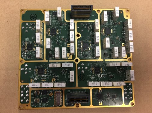
RF IC test PCBs are widely used for testing:
-
5G and cellular RF transceivers
-
Wi-Fi, Bluetooth, and IoT RF ICs
-
Automotive radar and V2X RF devices
-
Satellite and aerospace RF ICs
-
High-frequency analog and mixed-signal ICs
These applications demand high accuracy, repeatability, and stable RF performance.
Manufacturing Capabilities for RF IC Test PCBs
Producing reliable RF IC test PCBs requires advanced manufacturing capabilities, including:
-
Controlled impedance fabrication and RF verification
-
Low-loss, high-frequency laminate processing
-
HDI and multilayer PCB manufacturing
-
Precision drilling and RF connector assembly
-
Prototype, small batch, and volume production support
Advanced fabrication ensures consistent RF performance across test platforms.
Why RF IC Test PCB Quality Matters
A poorly designed RF IC test PCB can introduce signal attenuation, phase errors, and noise, resulting in inaccurate RF measurements and reduced yield. High-quality RF test PCBs provide:
-
Accurate RF parameter measurement
-
Reduced signal loss and reflection
-
Improved test repeatability and stability
-
Higher ATE efficiency and throughput
Conclusion
The RF IC Test PCB is a critical foundation for high-frequency semiconductor testing, enabling precise validation of RF IC performance. Through controlled impedance routing, low-loss materials, optimized grounding, and advanced manufacturing, RF IC test PCBs ensure reliable, repeatable, and accurate RF testing results.
Choosing an experienced RF IC test PCB manufacturer helps accelerate RF IC development, improve test accuracy, and ensure long-term reliability in wireless and high-frequency applications.
