An RF-35 PCB is a printed circuit board built using Taconic RF-35 laminate, a ceramic-filled PTFE-based material designed for high-frequency applications. With a dielectric constant of approximately 3.5 and a low dissipation factor, RF-35 provides a balance between signal performance, thermal stability, and manufacturability.
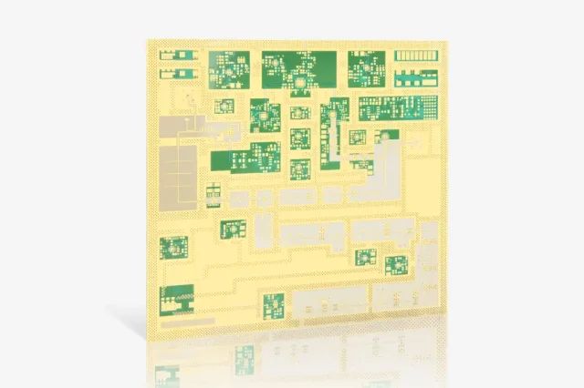
Compared to standard FR-4, RF-35 significantly reduces signal loss at high frequencies. At the same time, it is more cost-effective and easier to process than some ultra-high-end PTFE laminates, making it a popular choice for RF and microwave designs.
RF-35 PCBs are widely used in:
-
Wireless communication systems
-
RF modules and antennas
-
Microwave circuits
-
High-frequency test equipment
Material Characteristics
RF-35 laminates offer several advantages for high-frequency PCB design:
-
Low Dielectric Loss:
The low dissipation factor (Df) minimizes signal attenuation, ensuring efficient transmission in GHz-frequency applications. -
Stable Dielectric Constant (Dk ≈ 3.5):
Provides predictable impedance control across varying frequencies, which is critical for RF circuit design. -
Thermal Stability:
The ceramic-filled PTFE structure improves dimensional stability and thermal performance compared to pure PTFE materials. -
Moisture Resistance:
Low moisture absorption helps maintain electrical performance in humid or harsh environments. -
Mechanical Reliability:
Improved rigidity compared to traditional PTFE materials enhances handling and fabrication consistency.
Design Considerations
Designing RF-35 PCBs requires careful attention to RF-specific parameters:
-
Controlled Impedance Routing:
Microstrip, stripline, and coplanar waveguide structures are used to maintain consistent impedance and minimize reflections. -
Trace Optimization:
Short trace lengths, smooth curves, and minimal discontinuities help reduce insertion loss and signal distortion. -
Via Design:
Minimizing via transitions and using via stitching improves grounding and reduces impedance discontinuities. -
Grounding Strategy:
Solid ground planes and RF shielding techniques are essential for reducing EMI and maintaining signal integrity. -
Hybrid Stack-Ups:
RF-35 is often combined with FR-4 in multilayer designs to optimize cost while maintaining high-frequency performance.
Fabrication & Reliability
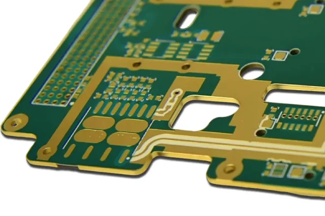
Although RF-35 offers improved manufacturability over pure PTFE materials, it still requires controlled processes:
-
Drilling and Hole Preparation:
Special handling ensures clean via walls and avoids substrate damage. -
Copper Adhesion:
Surface treatment is critical to ensure strong bonding between copper and PTFE-based laminate. -
Lamination Control:
Precise temperature and pressure profiles maintain layer alignment and dielectric consistency. -
Surface Finishes:
ENIG, immersion silver, or hard gold finishes are commonly used to support RF performance and durability. -
Quality Assurance:
-
Impedance testing for RF traces
-
Vector Network Analysis (VNA) for insertion and return loss
-
AOI/X-ray inspections for multilayer accuracy
-
Environmental testing for humidity and thermal stability
-
KKPCB applies strict process control to ensure RF-35 PCBs meet the performance and reliability requirements of RF and microwave systems.
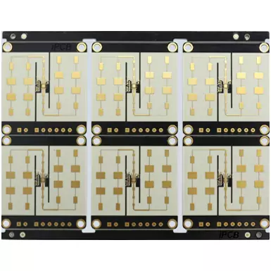
Applications
RF-35 PCBs are widely used in systems requiring stable, low-loss RF performance at a reasonable cost:
-
Wireless Communication: Antennas, RF front-end modules, and base stations
-
Microwave Systems: Filters, couplers, and amplifiers
-
Automotive Radar: Mid-frequency radar and sensing modules
-
Test & Measurement Equipment: RF signal generators and analyzers
-
Industrial RF Systems: Wireless control and monitoring devices
By combining low-loss dielectric properties, stable performance, and cost-effective processing, KKPCB delivers RF-35 PCBs that meet the demands of modern RF and high-frequency electronic applications.
