What is a PTFE PCB?
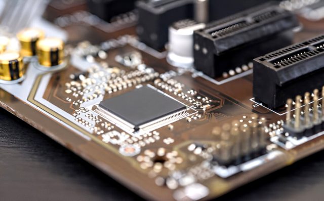
A PTFE PCB is a printed circuit board built using polytetrafluoroethylene (PTFE) as the substrate. PTFE is a high-performance polymer renowned for its extremely low dielectric loss (Df), consistent dielectric constant (Dk), and high thermal stability. These characteristics make PTFE PCBs ideal for applications where high-frequency signal integrity and minimal attenuation are critical.
Compared to conventional FR-4 boards, PTFE PCBs excel in:
-
High-frequency communication circuits (RF, microwave, mmWave)
-
Signal-sensitive measurement devices
-
Aerospace and defense electronics
-
High-speed test equipment
PTFE maintains stable electrical and mechanical properties over wide temperature ranges and under harsh operating conditions, making it the preferred choice for critical high-frequency designs.
PTFE PCB Design
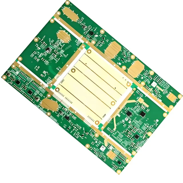
Designing PTFE PCBs requires careful attention to materials, trace geometry, and layout:
-
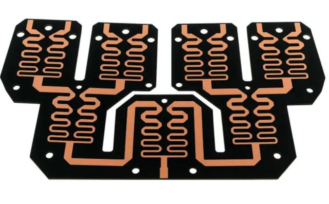
Transmission Line Optimization:
Traces are designed as controlled impedance transmission lines, using microstrip or stripline structures to minimize reflections and signal distortion. Precise control of trace width, spacing, and substrate thickness is critical. -
Low-Loss Routing:
PTFE’s ultra-low Df ensures minimal signal attenuation, which is essential for RF signals above 1 GHz. High-density layouts must be carefully routed to prevent crosstalk and maintain consistent performance across the board. -
Thermal and Mechanical Considerations:
PTFE is softer than FR-4 and prone to deformation under mechanical stress. Designers often use glass-filled or ceramic-reinforced PTFE to improve dimensional stability. Thermal vias and copper pours help dissipate heat from high-power or high-density areas. -
Hybrid Layer Stack-Up:
In many designs, PTFE layers are combined with standard FR-4 to optimize cost while preserving RF performance where critical. Stack-up planning also addresses impedance control and signal isolation.
Manufacturing Considerations and QA
PTFE PCB fabrication demands advanced processing:
-
Via Formation and Copper Adhesion: PTFE’s low surface energy requires special treatments to ensure strong copper adhesion. Laser or mechanical drilling is used for precision microvias.
-
Controlled Lamination: Temperature and pressure during lamination must be precisely managed to avoid delamination or warping.
-
Surface Finish Selection: ENIG, hard-gold, or immersion silver finishes are chosen to optimize solderability and RF performance.
-
Inspection and Testing:
-
Impedance Testing: Validates that traces meet design specifications
-
Vector Network Analysis (VNA): Measures return loss, insertion loss, and signal integrity
-
X-ray and AOI: Ensures via connectivity and multilayer alignment
-
Thermal Cycling: Confirms mechanical and electrical stability under operational stress
-
KKPCB leverages these processes to consistently deliver PTFE PCBs with high yield and reliable high-frequency performance.
Applications of PTFE PCBs
PTFE PCBs are widely used in demanding high-frequency environments:
-
5G and Wireless Communication: RF front-end modules, antennas, and mmWave devices
-
Aerospace and Defense: Satellite electronics, radar systems, and avionics
-
High-Speed Testing Equipment: Ensuring accurate signal transmission for test and measurement modules
-
RF Amplifiers and Microwave Circuits: Maintaining low-loss performance across critical signal paths
By combining precise layout, advanced low-loss PTFE materials, optimized thermal management, and rigorous QA, KKPCB delivers PTFE PCB solutions capable of reliable, high-performance operation in RF and microwave electronics.
