Introduction to PTFE PCB
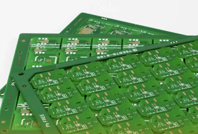
A PTFE PCB is a high-frequency printed circuit board manufactured using polytetrafluoroethylene-based laminate materials. PTFE is widely known for its extremely low dielectric loss and highly stable electrical performance at microwave and millimeter-wave frequencies.
As communication systems move into higher GHz ranges, substrate performance becomes a defining factor in overall signal quality. PTFE materials are specifically engineered to maintain signal integrity where conventional materials begin to degrade.
Why PTFE Performs Better at High Frequencies
At RF and microwave frequencies, signal energy interacts strongly with the dielectric material. The two most critical parameters are:
-
Dielectric constant (Dk)
-
Dissipation factor (Df)
PTFE offers:
-
Very low dissipation factor (minimizing insertion loss)
-
Stable dielectric constant across wide frequency ranges
-
Minimal signal dispersion
-
Reduced phase variation
These properties are especially valuable in circuits operating above 10GHz.
Electrical and Thermal Characteristics
1. Ultra-Low Dielectric Loss
PTFE significantly reduces energy loss as signals travel through transmission lines. This improves:
-
Signal amplitude retention
-
Power efficiency in RF amplifiers
-
Transmission distance in antenna feed structures
2. Stable Impedance Performance
Consistent dielectric properties allow:
-
Accurate 50Ω impedance control
-
Reliable differential routing
-
Stable return loss performance
This is critical for RF filters, couplers, and matching networks.
3. Wide Temperature Stability
PTFE materials maintain performance across wide temperature ranges and resist moisture absorption, making them suitable for outdoor and aerospace systems.
Manufacturing Challenges of PTFE PCB
While PTFE provides superior electrical performance, it presents unique fabrication challenges:
-
Soft material structure requiring controlled drilling
-
Higher coefficient of thermal expansion (CTE)
-
Special surface treatment for copper adhesion
-
Dedicated lamination profiles
Professional process control is necessary to ensure dimensional stability and reliable plating quality.
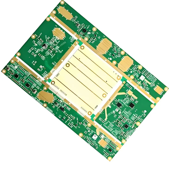
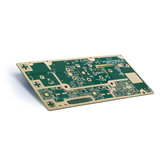
Structural Configurations
PTFE PCBs are available in:
-
Single-layer RF boards
-
Double-layer microwave circuits
-
Multilayer PTFE constructions
-
Hybrid stack-ups (PTFE + FR4)
-
Controlled impedance multilayer systems
Hybrid designs are commonly used to optimize cost while preserving RF performance in critical signal layers.
Typical Applications of PTFE PCB
PTFE PCBs are widely used in:
-
5G base station RF modules
-
Automotive radar (24GHz / 77GHz)
-
Satellite communication systems
-
Phased array antennas
-
Microwave test fixtures
-
Military RF equipment
-
Millimeter-wave transceiver modules
As system frequencies move into millimeter-wave bands, PTFE substrates become increasingly important.
PTFE PCB vs FR4 PCB
| Feature | FR4 PCB | PTFE PCB |
|---|---|---|
| Dielectric Loss | Higher | Extremely Low |
| Frequency Capability | Moderate | High / mmWave |
| Impedance Stability | Moderate | Excellent |
| Fabrication Complexity | Low | Higher |
| Cost | Lower | Higher |
PTFE PCB is selected when electrical performance outweighs cost and processing simplicity.
Conclusion
PTFE PCB technology provides ultra-low loss and highly stable dielectric performance required for modern RF and millimeter-wave systems. Although fabrication requires specialized handling, the electrical advantages make PTFE an essential material platform for high-frequency communication, radar, and aerospace applications.
As wireless systems continue to evolve toward higher frequencies and greater power density, PTFE PCB solutions remain a key enabler of reliable RF transmission.
