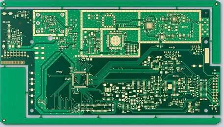
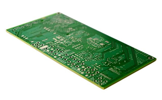
A Multilayer PCB is a printed circuit board that contains three or more conductive layers, allowing designers to manage complex circuitry in a compact space. As electronic systems become more sophisticated, multilayer PCBs have become essential for applications requiring high-speed signal routing, dense component placement, and reliable power distribution.
Multilayer PCBs are widely used in semiconductor test boards, RF and microwave systems, automotive electronics, 5G communication, medical devices, and industrial control systems, where performance, reliability, and space efficiency are critical.
Key Features of Multilayer PCBs
1. Multiple Signal, Power, and Ground Layers
Multilayer PCBs separate signal, power, and ground layers to reduce crosstalk, improve EMI performance, and maintain signal integrity in complex designs.
2. HDI and Microvia Integration
Advanced multilayer PCBs utilize HDI technology, blind/buried vias, and microvias, enabling higher routing density and fine pitch support for modern ICs.
3. Controlled Impedance Routing
High-speed digital and RF applications require precise impedance control. Multilayer PCBs provide consistent impedance for differential pairs, high-speed buses, and RF traces.
4. Compact Form Factor
By stacking multiple layers, multilayer PCBs allow designers to fit complex circuitry into smaller boards without sacrificing performance.
5. Enhanced Mechanical and Thermal Stability
With robust lamination processes, multilayer PCBs maintain mechanical strength and thermal reliability, essential for automotive, aerospace, and industrial applications.
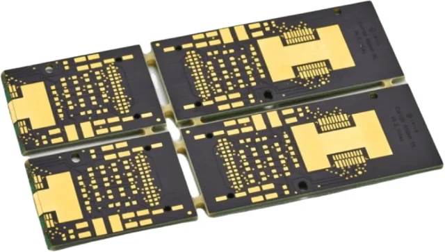
Applications of Multilayer PCBs
Multilayer PCBs are widely applied in:
-
Semiconductor test boards (ATE, probe cards, load boards)
-
High-speed digital and mixed-signal electronics
-
RF and microwave communication systems
-
5G base stations and mmWave modules
-
Automotive electronics and ADAS modules
-
Medical devices and industrial automation
These applications demand reliable signal integrity, compact design, and high manufacturing precision.
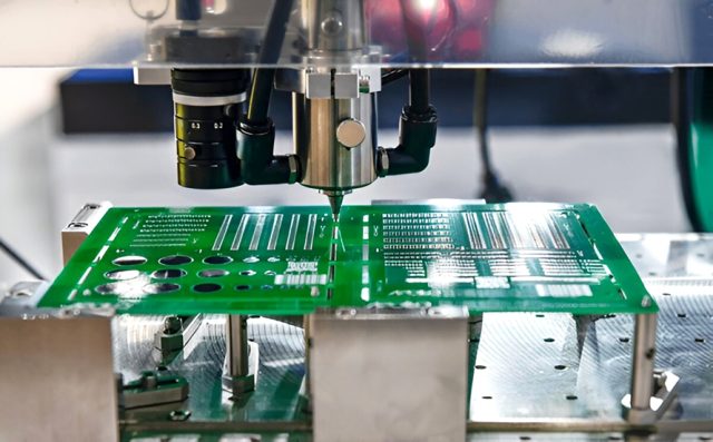
Manufacturing Requirements for Multilayer PCBs
Producing high-quality multilayer PCBs requires:
-
Precise lamination and alignment control
-
High-density HDI via and microvia processing
-
Controlled impedance verification
-
Multilayer stackup design optimization
-
Support for prototype, small batch, and volume production
Strict quality control ensures consistent electrical performance, high yield, and long-term reliability.
Why Multilayer PCB Quality Matters
Poorly manufactured multilayer PCBs can result in:
-
Crosstalk and signal degradation
-
Impedance mismatch and RF loss
-
Reduced test yield and product reliability
-
Mechanical warping and thermal failure
High-quality multilayer PCBs ensure stable signal transmission, reliable power delivery, and consistent performance in advanced electronic systems.
Conclusion
The Multilayer PCB is a critical technology for modern electronics, enabling complex circuitry, high-speed performance, and compact form factors. Through HDI integration, controlled impedance routing, optimized multilayer stackups, and precise manufacturing, multilayer PCBs deliver high-quality, reliable solutions for high-performance applications.
Partnering with an experienced multilayer PCB manufacturer ensures efficient product development, improved yield, and long-term system reliability.
