Multilayer PCB: Advanced Design for High-Density and High-Speed Electronics
With modern electronic devices becoming increasingly compact and high-performance, Multilayer PCB technology is essential for achieving complex circuit routing, improved signal integrity, and efficient power distribution. A multilayer PCB consists of three or more conductive copper layers laminated together with dielectric materials , enabling compact, high-density, and high-speed electronic designs.
Multilayer PCBs are widely used in telecommunications, automotive systems, industrial control, medical devices, and high-speed computing applications.
What Is a Multilayer PCB?
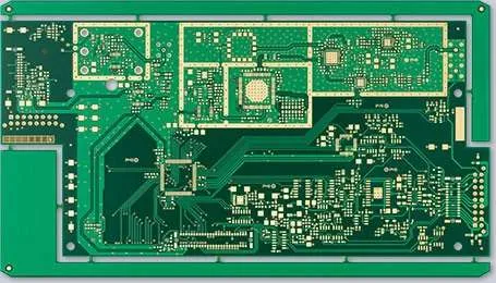
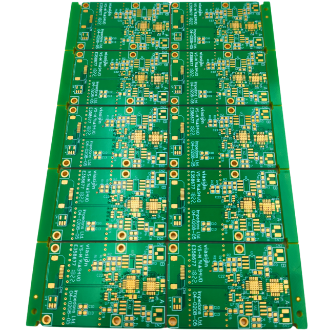
A Multilayer PCB is a printed circuit board made up of multiple copper layers separated by insulating prepreg and core materials. Unlike single-sided or double-sided PCBs, multilayer boards provide additional routing layers, which allow complex circuitry in a compact footprint.
Common multilayer configurations include:
-
4-layer PCB
-
6-layer PCB
-
8-layer PCB
-
10-layer and above for advanced applications
The number of layers is determined by routing complexity, power distribution, EMI/EMC requirements, and impedance control for high-speed signals.
Advantages of Multilayer PCBs
1. High Circuit Density
Multiple layers allow designers to route complex circuits in limited board space, ideal for compact devices such as smartphones, tablets, and IoT electronics.
2. Improved Signal Integrity
Dedicated ground and power planes reduce crosstalk, minimize noise, and maintain stable high-speed signal performance.
3. Controlled Impedance
Advanced multilayer stackups enable precise impedance control for high-speed digital and RF PCB applications.
4. Better Thermal Management
Internal copper planes and optimized layer distribution help dissipate heat from high-power devices.
5. Enhanced Mechanical Strength
The laminated structure increases rigidity and durability, critical for automotive, industrial, and aerospace electronics.
Design Considerations for Multilayer PCB
Effective multilayer PCB design requires attention to:
-
Layer stackup and symmetry to avoid warpage
-
Dielectric material selection for stable electrical performance
-
Copper thickness for current-carrying capability
-
Via design, including through-hole, blind, and buried vias
-
Impedance control for high-speed circuits
Collaboration with PCB manufacturers ensures optimal manufacturability and performance.
Applications of Multilayer PCBs
Multilayer PCBs are essential in high-density and high-speed electronics, including:
-
Telecommunication equipment (5G, servers, routers)
-
Automotive electronics (ADAS, EV controllers, infotainment)
-
Medical devices (imaging, monitoring systems)
-
Industrial automation (PLC systems, robotics)
-
Consumer electronics (smartphones, laptops, wearables)
In high-frequency applications, multilayer PCBs maintain signal integrity and reliability.
Manufacturing Process
The multilayer PCB fabrication process involves:
-
Inner layer imaging and etching
-
Layer alignment and lamination
-
Drilling and via metallization
-
Outer layer patterning
-
Surface finishing (ENIG, HASL, OSP, etc.)
-
Electrical testing and quality inspection
Precision in lamination and drilling ensures layer alignment and impedance consistency.
Conclusion
Multilayer PCB technology enables complex, high-density, and high-speed circuits in modern electronic devices. By optimizing stackups, materials, and via structures, multilayer PCBs improve signal integrity, thermal management, and mechanical strength, supporting advanced applications from consumer electronics to industrial systems.
