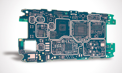
Why Microvias Are Critical in Modern PCB Design
As electronic devices continue to shrink while performance demands increase, traditional through-hole vias become a limiting factor. Microvias solve this by enabling high-density interconnects with shorter electrical paths.
They are essential when:
- BGA pitch ≤ 0.8 mm (especially ≤ 0.5 mm)
- Routing congestion limits layout feasibility
- High-speed signals require reduced parasitics
- Board size must be minimized
In these scenarios, microvias are not optional—they are a design enabler.
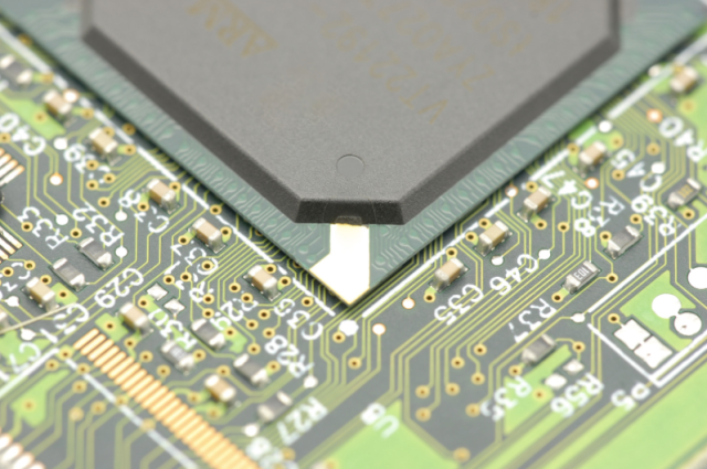
What Defines a Microvia? (Quick Technical Overview)
A microvia is a laser-drilled via, typically:
- Diameter: ≤150 µm
- Depth: connects only adjacent layers
- Structure: blind via (not through-hole)
Key differences from traditional vias:
| Feature | Microvia | Through Via |
|---|---|---|
| Size | Very small | Larger |
| Depth | Shallow | Full board |
| Parasitics | Low | Higher |
| Density | High | Limited |
This structural difference directly impacts signal integrity and routing capability.
Microvia Structures & When to Use Them
Choosing the right structure is a critical engineering decision:
1. Single Microvia (1+N+1)
- Most stable and cost-effective
- Ideal for moderate HDI designs
2. Staggered Microvia
- Offset between layers
- Better reliability than stacked
- Recommended for most designs
3. Stacked Microvia
- Vertically aligned
- Enables maximum density
- Higher cost and reliability risk
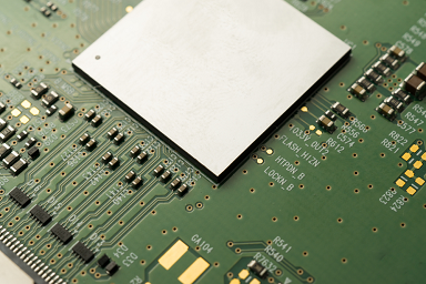
4. Via-in-Pad Microvia
- Placed directly under BGA pads
- Required for ultra-fine pitch packages
Key Insight:
Use the simplest structure that meets routing needs—not the most advanced one.
The Hidden Risk: Why Microvias Fail
Microvias improve density—but also introduce failure risks if poorly designed:
- Thermal Cycling Cracks
Expansion mismatch causes stress at via interfaces - Stacked Via Weak Points
Vertical stacking concentrates mechanical stress - Plating Defects
Thin or uneven copper reduces reliability - Void Formation
Incomplete filling weakens structure - Material Mismatch (CTE)
Causes fatigue under temperature variation
In high-reliability applications, microvia failure is one of the top PCB failure modes.
Practical Design Rules (What Actually Works)
Instead of theory, here are actionable engineering rules:
- Prefer staggered over stacked vias
- Limit stacking levels whenever possible
- Use via-in-pad only when necessary
- Maintain proper aspect ratio control
- Ensure filled & capped vias for reliability
- Keep stack-up symmetrical to reduce stress
- Collaborate early with PCB manufacturer (DFM)
Golden Rule:
Density should never compromise reliability.
Cost vs Performance: The Real Trade-Off
Microvias increase performance—but also cost.
Cost drivers include:
- Number of microvias
- Stacking complexity
- Lamination cycles
- Filling and plating processes
Engineering balance:
- Overdesign → unnecessary cost
- Underdesign → routing failure or SI issues
The goal is not maximum density, but optimal efficiency.
When Should You Choose Microvia PCB?
Use microvia PCBs when:
- Fine-pitch BGA routing is required
- High-speed performance demands low parasitics
- Board size constraints are strict
- Multilayer routing becomes inefficient
Avoid them when:
- Standard vias meet requirements
- Cost sensitivity is high
- Signal speeds are moderate
Final Thoughts
Microvia PCBs are a key technology for modern electronics, but they require careful engineering decisions.
The success of a microvia design depends on:
- Correct structure selection
- Reliability-focused design rules
- Balanced cost-performance decisions
- Strong manufacturing control
At KKPCB, we support microvia PCB development with advanced laser drilling, precision plating, and DFM collaboration, ensuring your HDI designs achieve both high performance and long-term reliability.
