Microvia PCB: High-Density Interconnect Solutions for Advanced Electronics
As electronic devices become smaller, faster, and more complex, designers face increasing challenges in routing high-density circuits. Microvia PCB technology provides a solution by enabling high-density interconnects (HDI), allowing for compact multilayer designs with superior electrical performance.
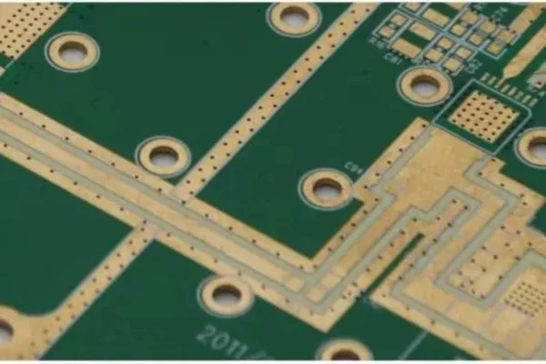
A Microvia PCB uses extremely small vias, typically less than 150 µm in diameter, to connect layers in a multilayer PCB. These microvias facilitate miniaturization, reduce signal interference, and improve overall PCB reliability, making them ideal for advanced consumer electronics, medical devices, telecommunications, and aerospace systems.
What Is a Microvia PCB?
A Microvia PCB is a printed circuit board that uses microvias instead of traditional through-hole vias to connect layers. Microvias are usually:
-
Laser-drilled for precision
-
Blind vias (connect outer layer to an inner layer)
-
Buried vias (connect only internal layers)
Microvias are smaller and shallower than standard vias, enabling more routing space and higher interconnect density in multilayer PCBs.
Advantages of Microvia PCB Technology
1. High-Density Interconnect (HDI)
Microvias allow more connections per unit area, supporting compact and complex PCB designs. They are widely used in smartphones, tablets, and wearable electronics.
2. Improved Signal Integrity
Shorter via lengths reduce parasitic inductance and capacitance, minimizing signal loss and enhancing high-speed signal performance.
3. Miniaturization
Microvia PCBs enable thinner boards and smaller footprints, which is critical for portable and embedded devices.
4. Enhanced Reliability
Smaller vias reduce thermal stress and mechanical strain on the board, improving long-term reliability.
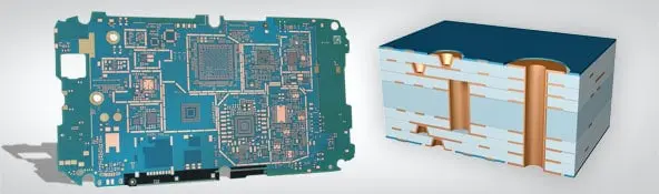
5. Multilayer Integration
Microvia technology allows the creation of multilayer PCBs with 6, 8, or even 12+ layers, providing higher routing density and functionality.
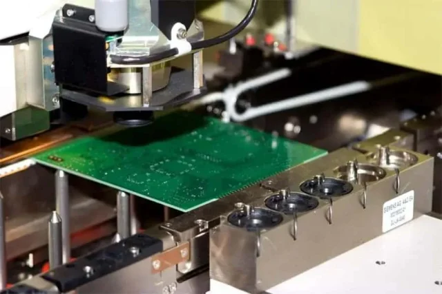
Microvia PCB Manufacturing Techniques
Creating microvia PCBs requires precise and advanced manufacturing processes:
-
Laser Drilling – Produces small, accurate vias without damaging surrounding material
-
Sequential Lamination – Stacks HDI layers with microvias to form complex multilayer boards
-
Copper Plating – Ensures reliable electrical connections within microvias
-
High-Resolution Imaging – Maintains fine trace width and spacing for HDI layouts
Design Considerations for Microvia PCBs
When designing a microvia PCB, engineers must consider:
-
Via diameter and aspect ratio – To ensure reliable plating and connectivity
-
Via density – Higher density allows more routing but increases manufacturing complexity
-
Stacked vs staggered microvias – Balances routing density with mechanical reliability
-
Trace width and spacing – Maintains signal integrity and manufacturability
-
Material selection – Low-loss laminates improve high-frequency performance
Proper planning and close collaboration with PCB manufacturers are essential for optimal performance.
Applications of Microvia PCB
Microvia PCBs are critical in applications that demand high density and miniaturization:
-
Smartphones and tablets
-
Wearable devices and IoT electronics
-
Medical imaging and monitoring devices
-
Telecommunications and networking equipment
-
Aerospace and defense electronics
-
High-speed computing and server boards
In these applications, microvia technology enables compact layouts without compromising performance or reliability.
Conclusion
Microvia PCB technology is a cornerstone of modern high-density and high-performance electronics. By using laser-drilled microvias and advanced HDI techniques, designers can achieve compact, reliable, and high-speed multilayer PCBs. As consumer electronics and industrial systems continue to miniaturize, microvia PCBs will remain essential for next-generation PCB design.
