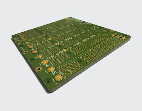
What is a Megtron PCB?

A Megtron PCB is a printed circuit board built using Megtron high-frequency laminates, developed to provide low dielectric loss (Df), stable dielectric constant (Dk), and excellent thermal performance for high-speed and high-frequency electronics.
Megtron laminates are commonly used in:
-
High-speed communication devices
-
RF and microwave circuits
-
Gigabit and multi-gigabit data transmission
-
High-frequency networking equipment
Compared to standard FR-4, Megtron PCBs reduce signal attenuation, maintain controlled impedance, and improve signal integrity in demanding applications.
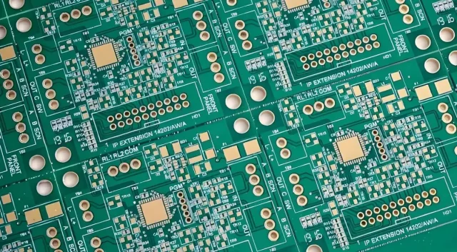
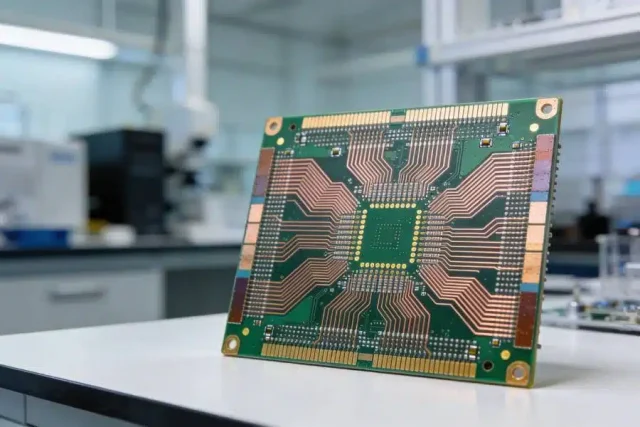
Megtron PCB Design
Designing Megtron PCBs requires attention to both electrical and thermal performance:
-
Controlled Impedance:
High-frequency signals require precise trace width and spacing. Megtron laminates allow designers to create microstrip and stripline traces with consistent impedance, minimizing reflections and signal distortion. -
Low-Loss Routing:
The ultra-low Df of Megtron materials reduces dielectric and conductor losses, which is critical for maintaining signal integrity at GHz-level frequencies. -
Thermal Management:
Megtron PCBs exhibit stable thermal characteristics. Proper layer stack-ups, thermal vias, and copper pours help manage heat in densely packed high-speed circuits. -
Layer Stack-Up and Crosstalk Reduction:
Multilayer Megtron PCBs separate high-speed signal layers from power and ground planes, reducing crosstalk and electromagnetic interference (EMI). -
Material Selection:
Different Megtron laminates (Megtron 6, Megtron 6.5) are chosen based on frequency range, insertion loss requirements, and thermal performance needs.
Manufacturing Considerations and QA
Fabrication of Megtron PCBs demands precision and stringent quality control:
-
Drilling and Plating: Laser or mechanical drilling ensures via quality without damaging low-loss substrates.
-
Controlled Lamination: Accurate temperature and pressure maintain dielectric consistency across layers.
-
Surface Finishes: ENIG, immersion silver, or hard-gold finishes are applied for reliability and signal performance.
-
Inspection and Testing:
-
Impedance verification for controlled transmission lines
-
Vector Network Analysis (VNA) to measure insertion loss and return loss
-
AOI and X-ray inspections to confirm multilayer and via integrity
-
KKPCB ensures all Megtron PCBs meet tight electrical specifications and are suitable for high-frequency deployment.
Applications of Megtron PCBs
Megtron PCBs are essential in applications requiring high-speed signal transmission and low-loss performance:
-
High-Speed Networking: Gigabit routers, switches, and optical communication modules
-
RF and Microwave Systems: Antennas, filters, and high-frequency transceivers
-
5G Communication: Base stations and RF front-end modules
-
Data Centers and Servers: High-speed signal distribution boards
-
Test & Measurement Equipment: High-frequency diagnostic and validation tools
By leveraging advanced Megtron laminates, precise trace design, thermal management, and rigorous QA, KKPCB delivers Megtron PCBs capable of reliable operation in demanding high-speed and high-frequency electronic systems.
